Interface Definitions

DC688 provides a rich set of interfaces, as shown below:
The images on this page are actual photos of the DC686. The DC688 and DC686 share the
Device Interface Definitions
Device interfaces
J1 TYPE-C Port
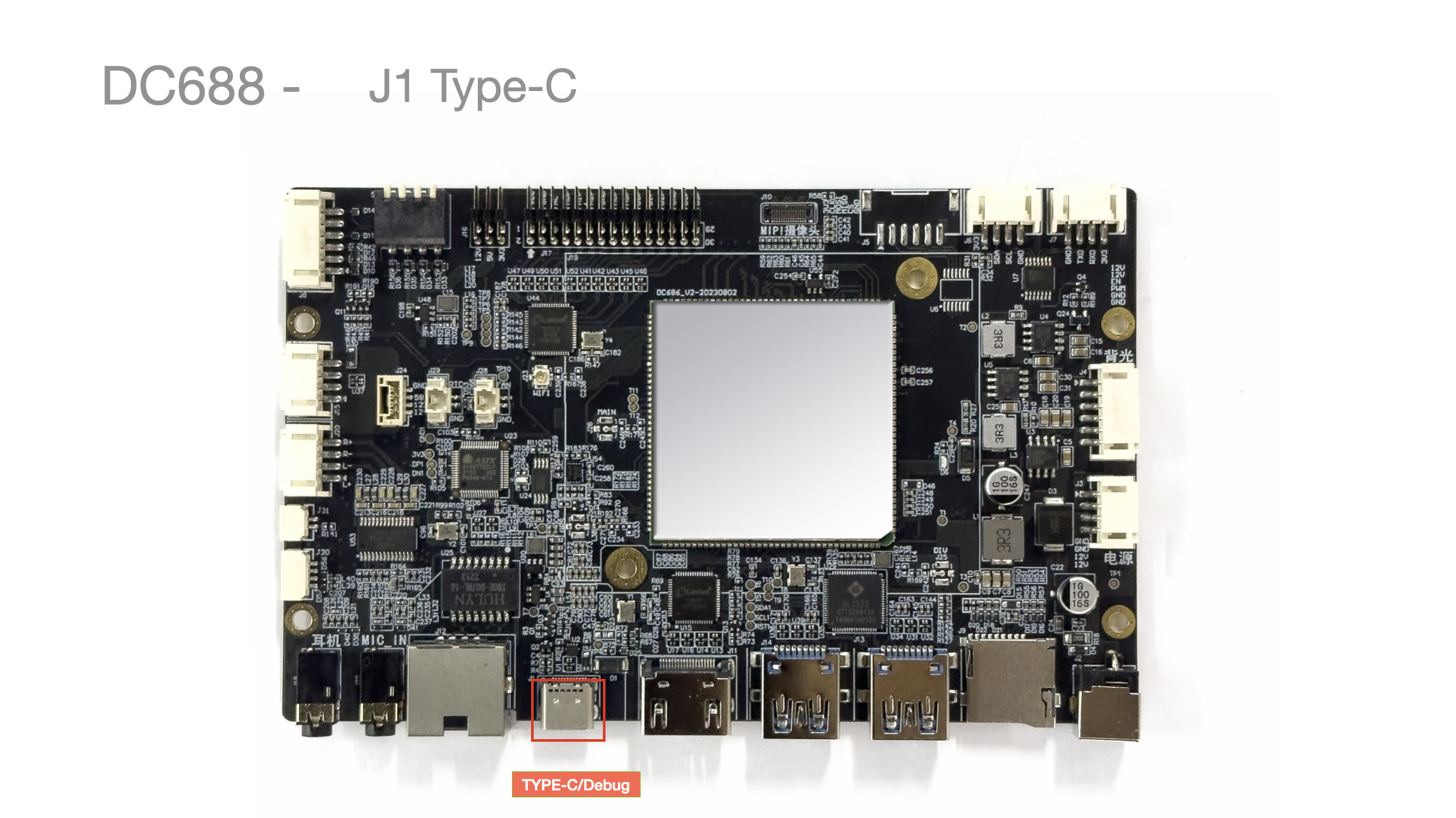
- TYPE-C port: Debug
J2/J3 Power
Connection method
Interface Definition
| Pin No. | Pin Description | Wire Color (Reference) | Remarks |
|---|---|---|---|
| 1 | GND | Black | Ground |
| 2 | GND | Black | Ground |
| 3 | 12V | Red | Operating voltage 12V |
| 4 | 12V | Red | Operating voltage 12V |
Just Connect a 12V Power Supply
- Supports a
DC 12V 4PINpower connector
Measured Power
-
Test method:
-
Flash the default
Androidfirmware -
Power on normally, unlock the screen and do nothing else
-
Only the mainboard power is measured; the backlight is not connected.
-
| Status | Voltage | Current | Power | Remarks |
|---|---|---|---|---|
| Normal boot without a screen connected | 12.4V | 0.2A | Standby 2.3-3.1W | Measurement accuracy 0.1, |
J4 Backlight Power
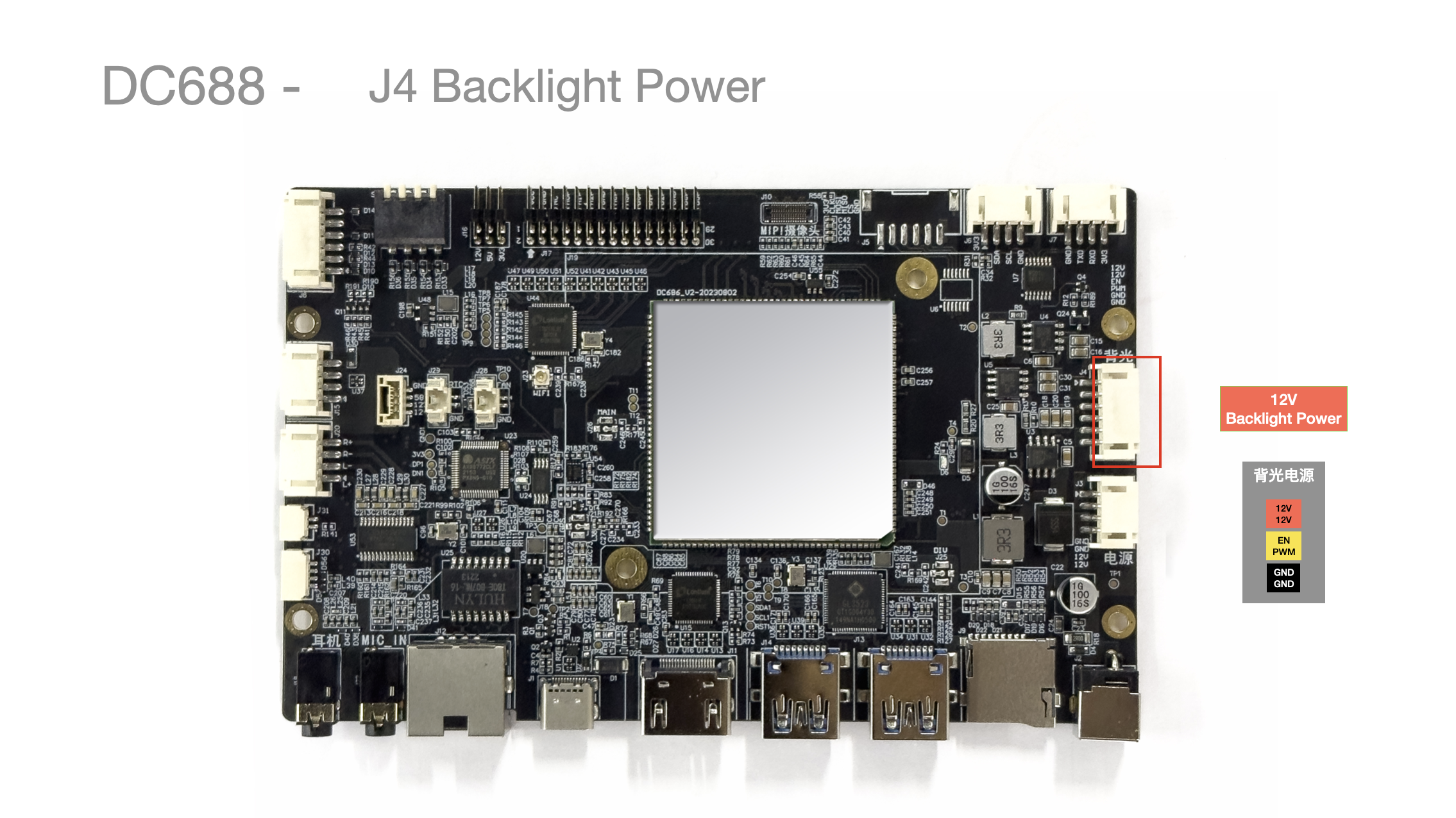
| Pin No. | Pin Description | Wire Color (Reference) | Remarks |
|---|---|---|---|
| 1 | 12V | Red | Operating voltage 12V |
| 2 | 12V | Red | Operating voltage 12V |
| 3 | BL EN | Yellow | Backlight control |
| 4 | BL PWM | Yellow | Backlight control |
| 5 | GND | Black | Ground |
| 6 | GND | Black | Ground |
- Maximum
3A Max
J5 SPI
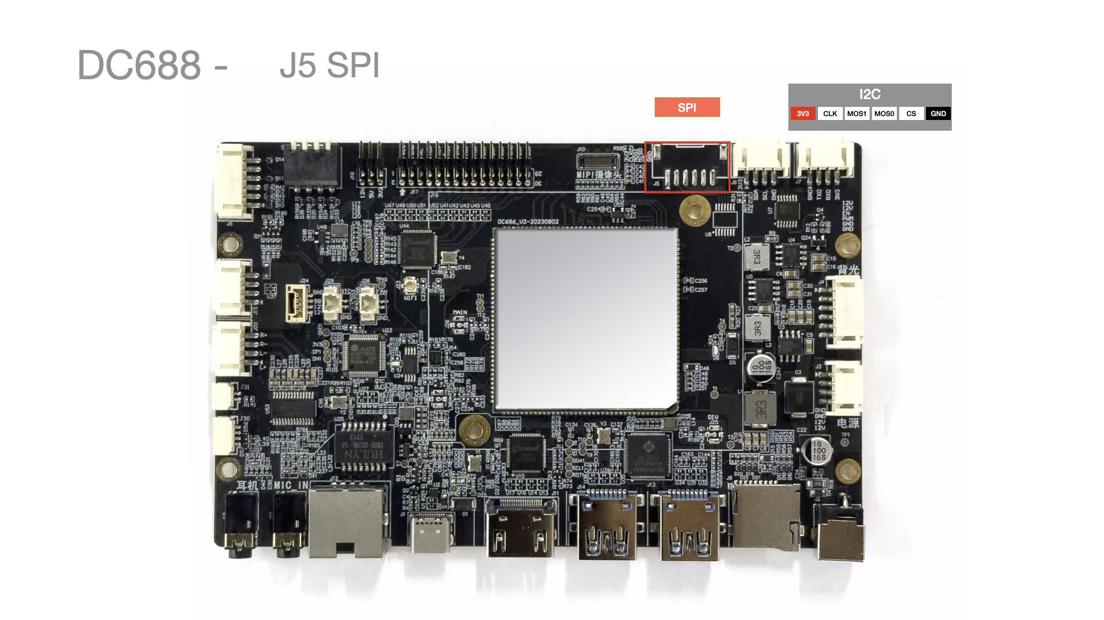
| Pin No. | Pin Description | Remarks |
|---|---|---|
| 1 | 3V3 | |
| 2 | SPI2_CLK_3 | |
| 3 | SPI2_MOSI_3 | |
| 4 | SPI2_MISO_3 | |
| 5 | SPI2_CS_3 | |
| 6 | GND |
J6 I2C
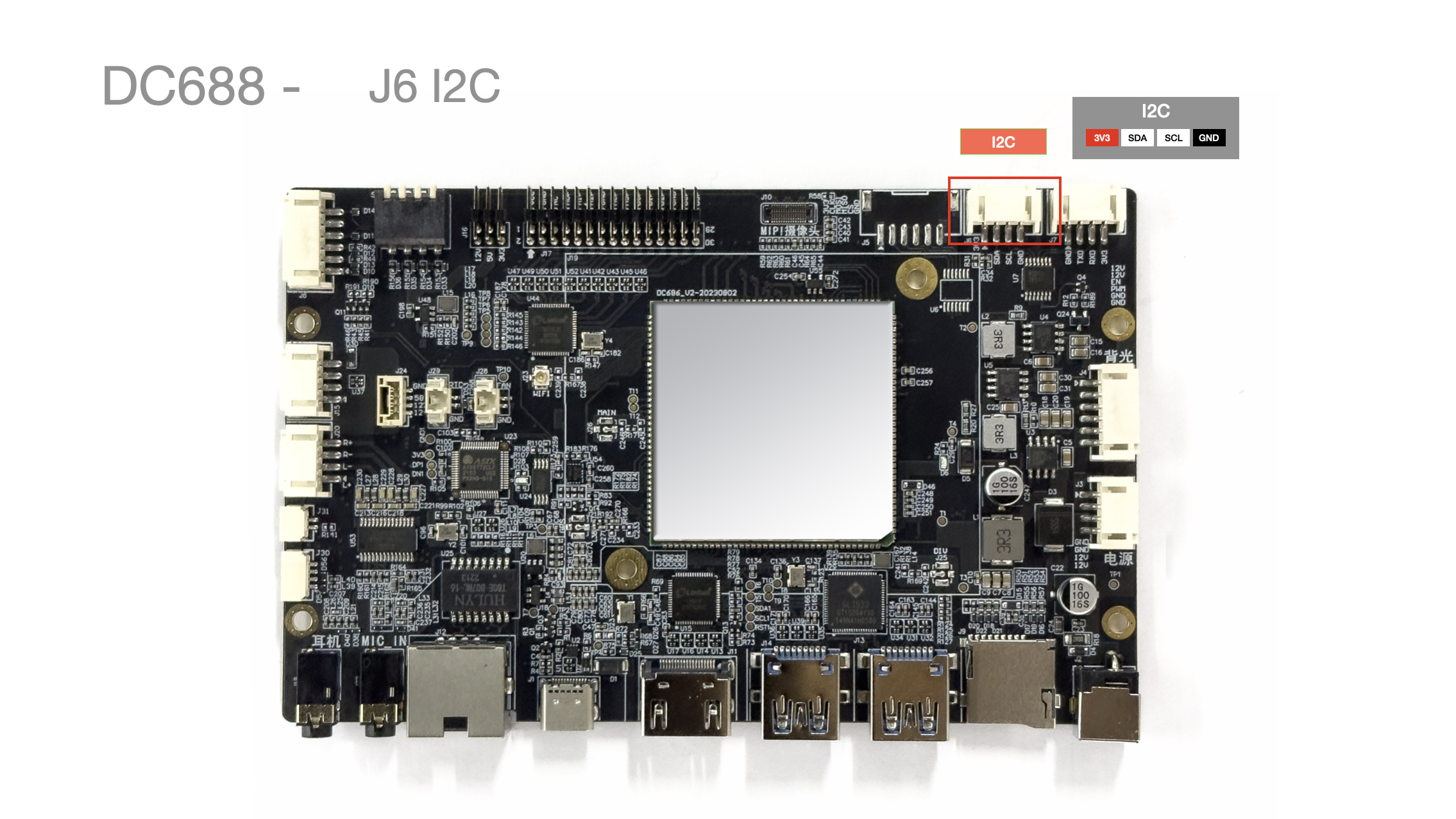
| Pin No. | Pin Description | Remarks |
|---|---|---|
| 1 | 3V3 | |
| 2 | TP_SDA_3 | |
| 3 | TP_SCL_3 | |
| 4 | GND |
J7 UART/Debug Interface
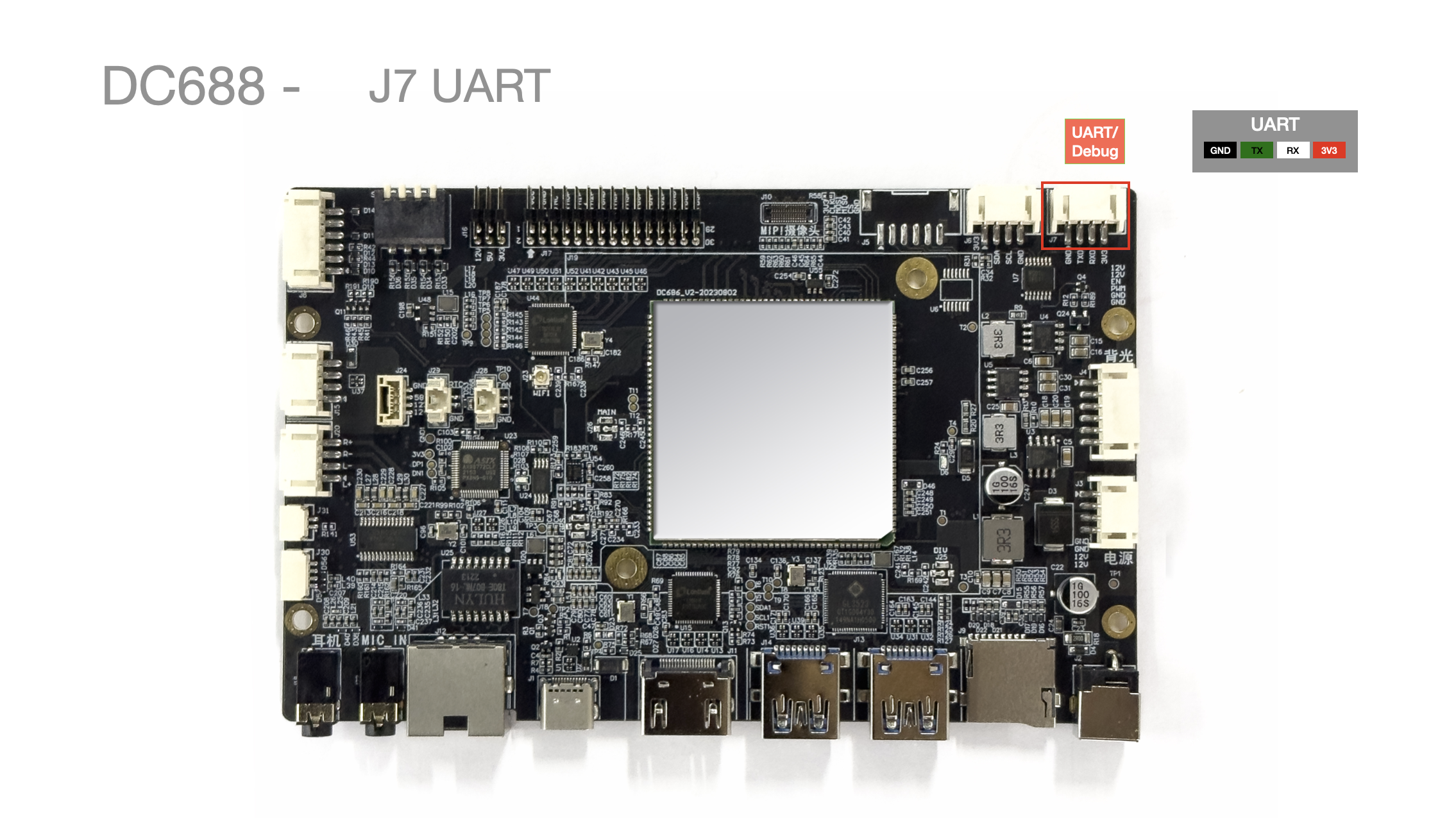
| Pin No. | Pin Description | Wire Color (Reference) |
|---|---|---|
| 1 | GND | Black |
| 2 | TX | Green |
| 3 | RX | White |
| 4 | 3V3 | Red |
J8 Panel Button Interface
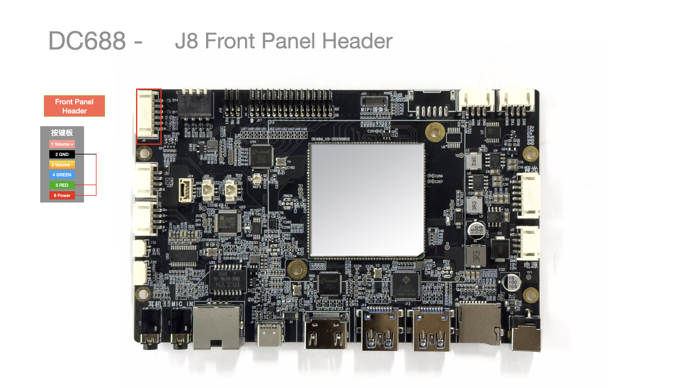
| Pin No. | Pin Description | Wire Color (Reference) | Remarks |
|---|---|---|---|
| 1 | Power | None | Short with 5 GND for the power button |
| 2 | GPIO57_3v3 | None | |
| 3 | GPIO44_3V3 | None | |
| 4 | Volume + | None | Short with 5 GND for volume - |
| 5 | GND | Black | Ground |
| 6 | Volume + | None | Short with 5 GND for volume + |
- Press and hold
Volume + during startup to enter Loader upgrade mode
J9 TF-Card Interface
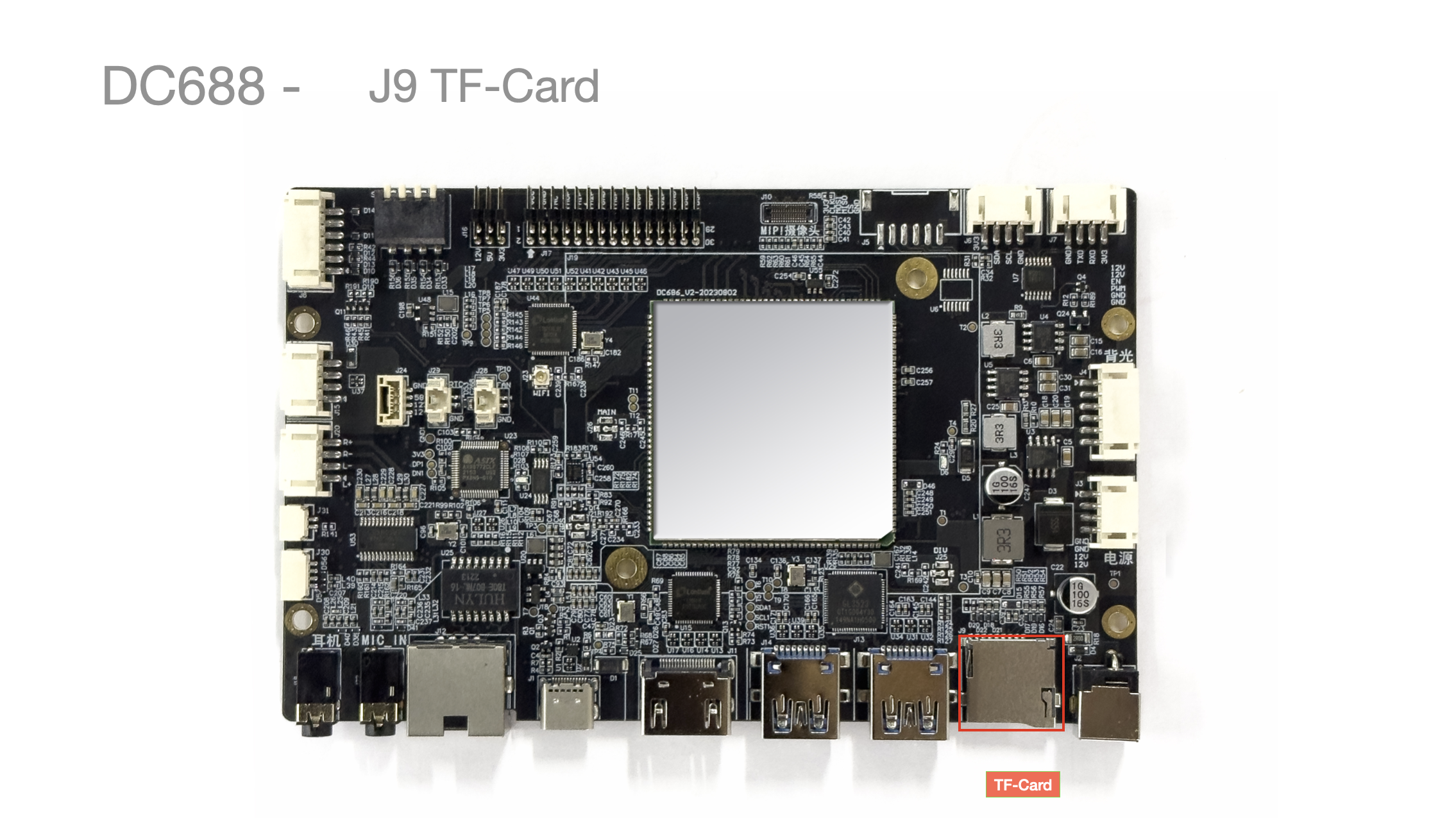
Measured maximum 256G; theoretically supports 512G
J10 MIPI Camera
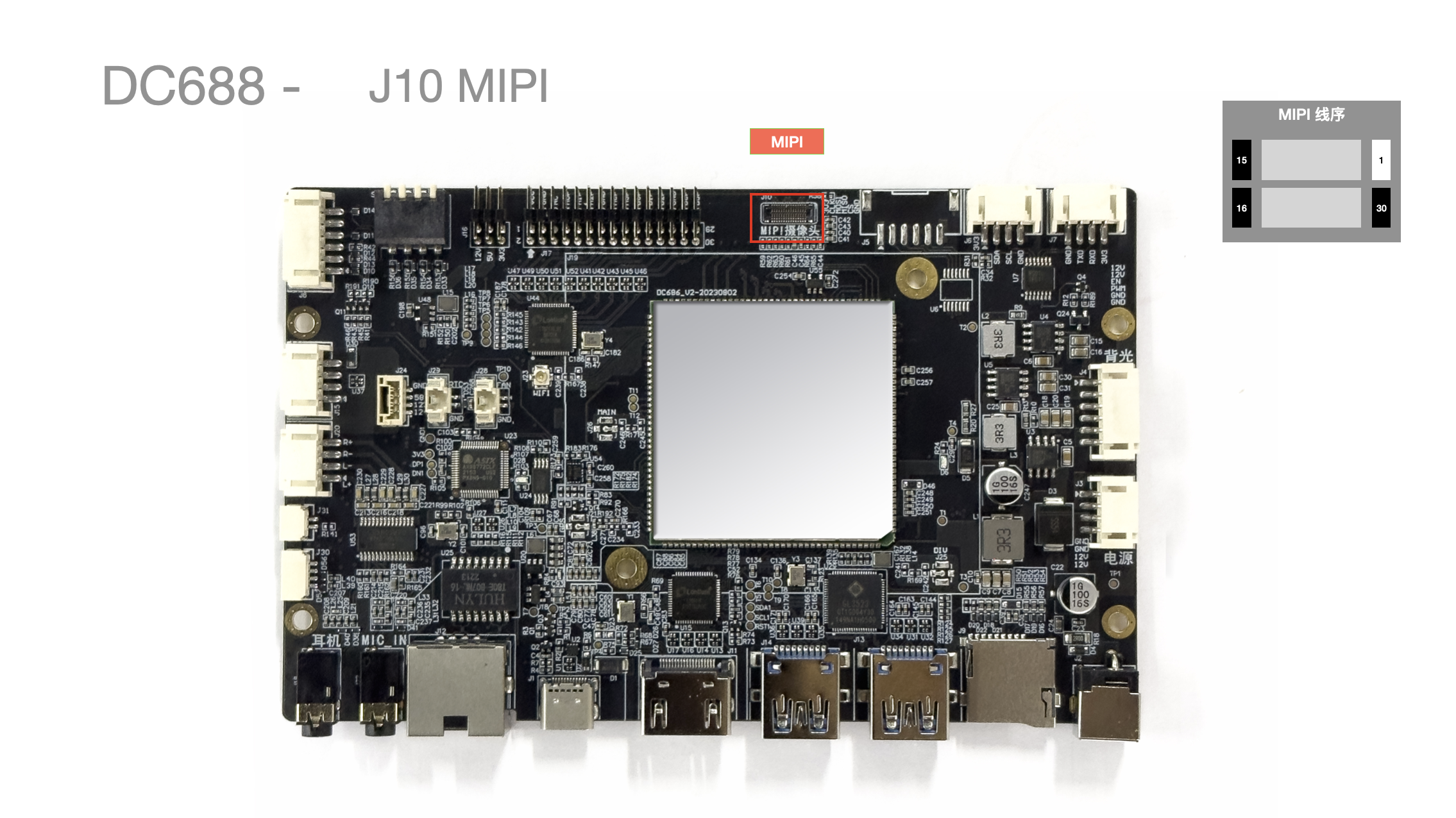
- Connector model: YXT-BB10-30S-02
J11 HDMI-IN Video Input
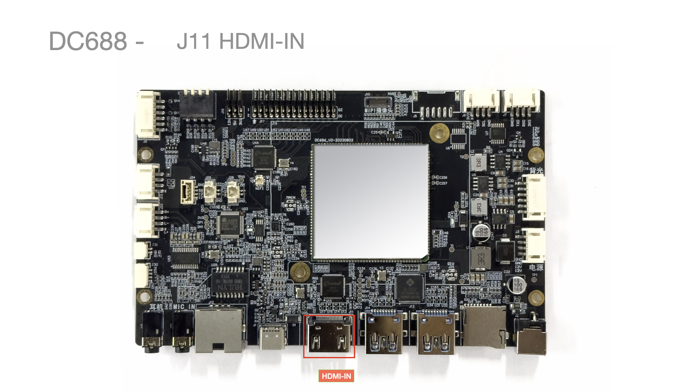
- 1xHDMI IN: supports resolutions 19201080@60/38402160@30
J12 Ethernet Interface
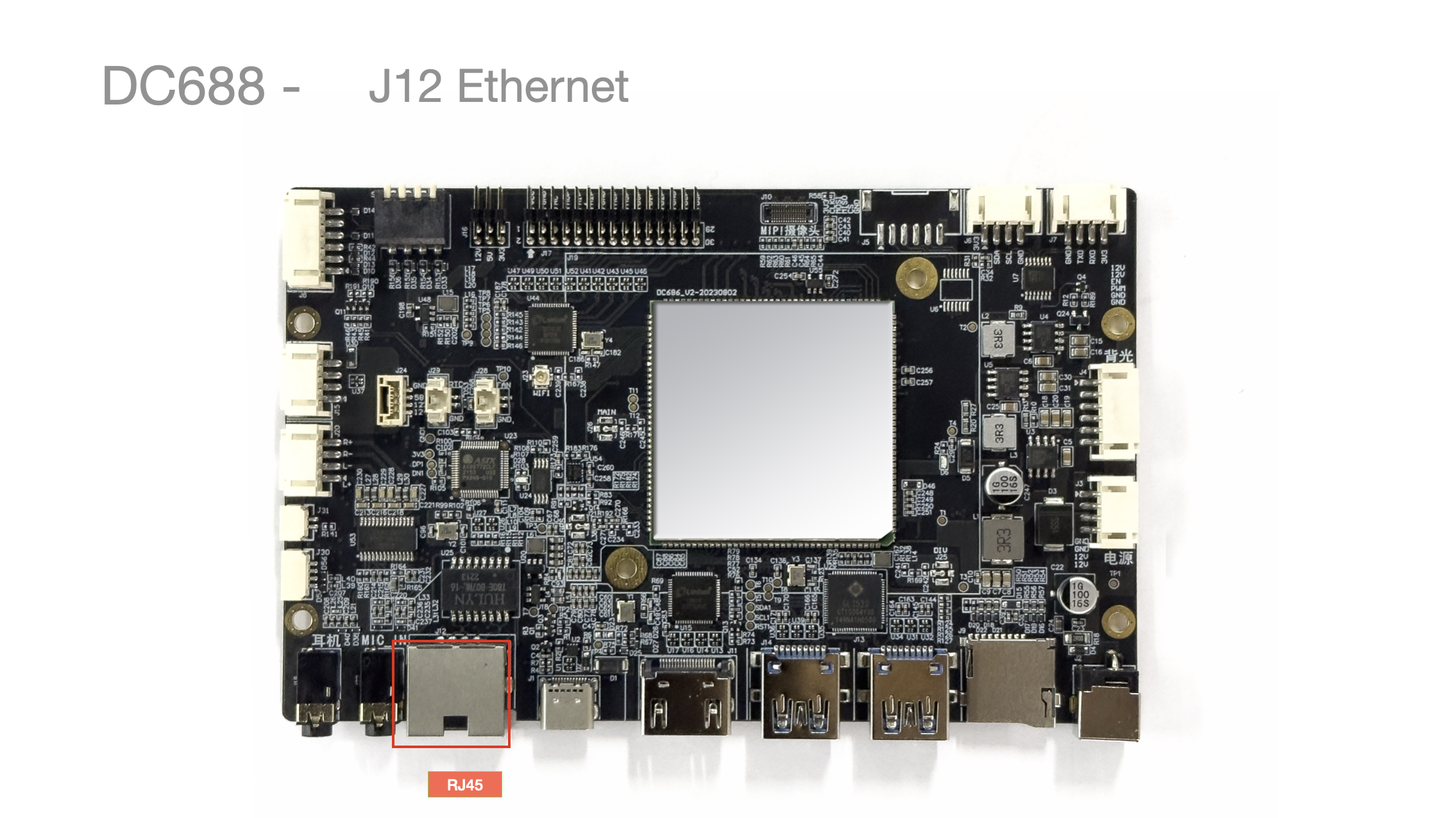
-
Auto-negotiating Gigabit Ethernet, supports 10/100/1000Mbps
-
J12 and J15 are output from the same USB HUB port, so
J12 USB and the J15 Ethernet port are mutually exclusive
J13/J14 USB-A 3.0 Interfaces
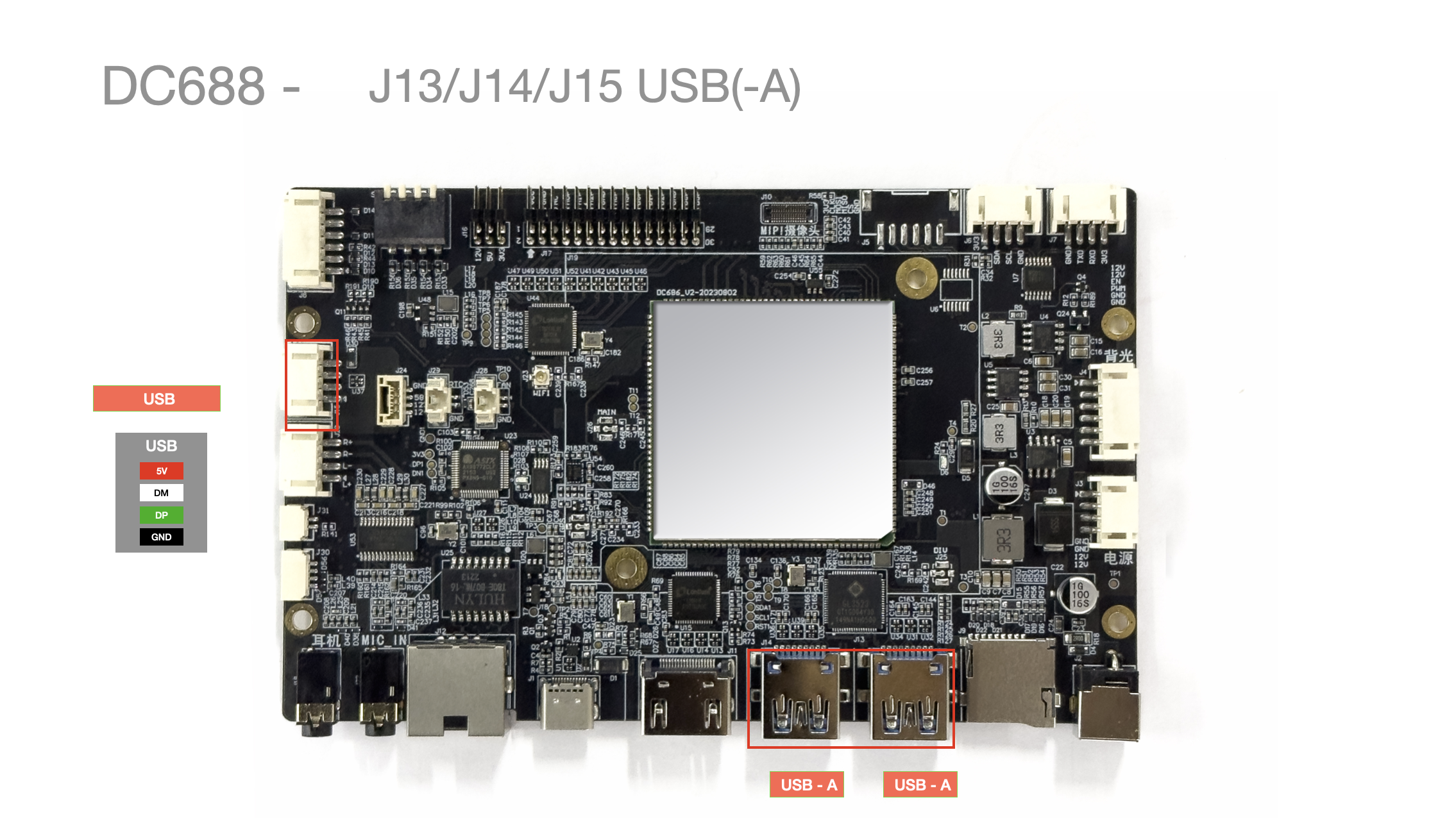
- Supports 2 USB-A 3.0 standard interfaces
J15 USB Interface
- Supports 1 USB PH2.0 4PIN channel
| Pin No. | Pin Description | Wire Color (Reference) | Remarks |
|---|---|---|---|
| 1 | GND | Black | Ground |
| 2 | DP | Green | |
| 3 | DM | White | |
| 4 | 5V | Red | 5V |
J16 LVDS Power Selection
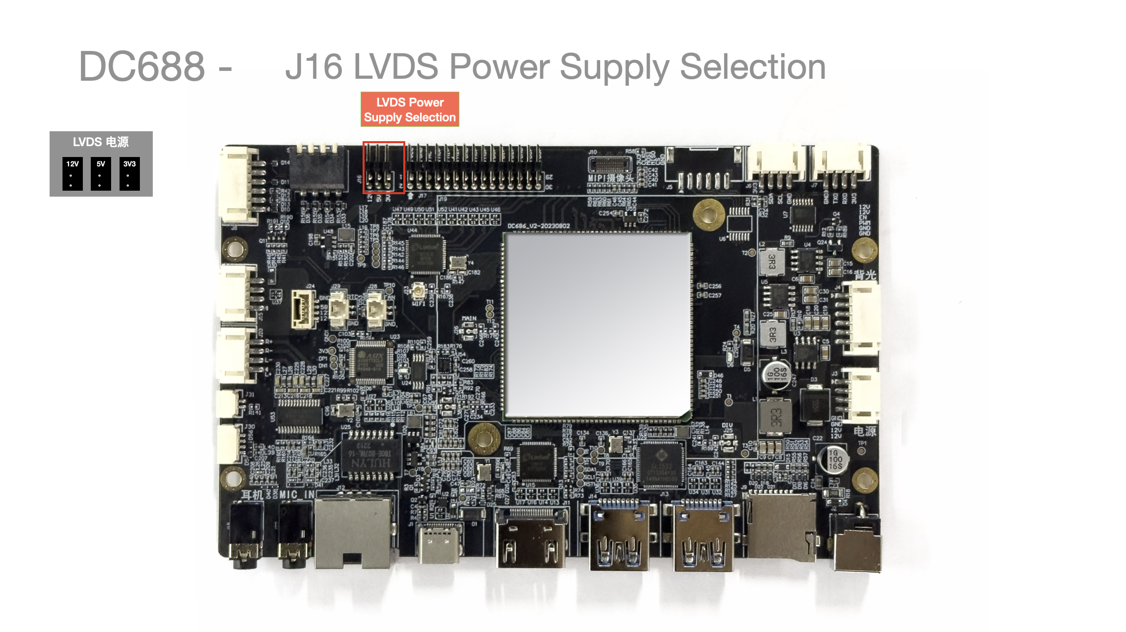
- Pay attention to the
output voltage to avoiddamaging the screen
J17 LVDS Interface
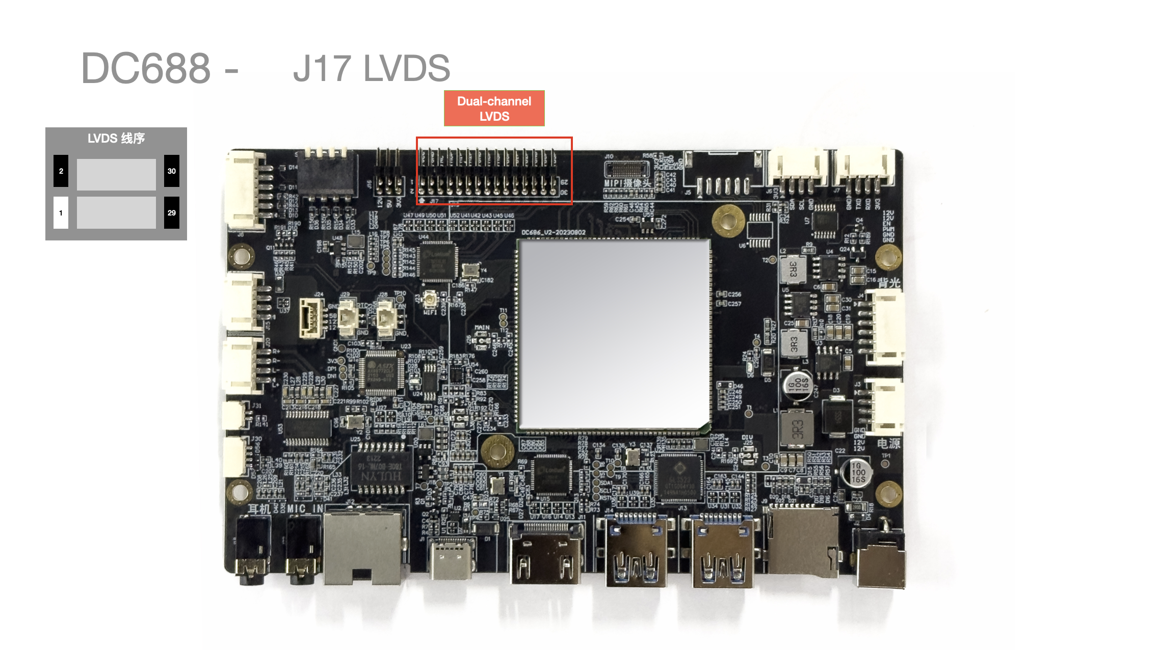
- LVDS interface
| Pin No. | Pin Description |
|---|---|
| 1 | LVDS1_VCC |
| 2 | LVDS1_VCC |
| 3 | GND |
| 4 | LVDS1_VCC |
| 5 | NC |
| 6 | GND |
| 7 | LVDS1A_Y0P |
| 8 | LVDS1A_Y0N |
| 9 | LVDS1A_Y1P |
| 10 | LVDS1A_Y1N |
| 11 | LVDS1A_Y2P |
| 12 | LVDS1A_Y2N |
| 13 | GND |
| 14 | GND |
| 15 | LVDS1A_CLK_P |
| 16 | LVDS1A_CLK_N |
| 17 | LVDS1A_Y3P |
| 18 | LVDS1A_Y3N |
| 19 | LVDS1B_Y0P |
| 20 | LVDS1B_Y0N |
| 21 | LVDS1B_Y1P |
| 22 | LVDS1B_Y1N |
| 23 | LVDS1B_Y2P |
| 24 | LVDS1B_Y2N |
| 25 | GND |
| 26 | GND |
| 27 | LVDS1B_CLK_P |
| 28 | LVDS1B_CLK_N |
| 29 | LVDS1B_Y3P |
| 30 | LVDS1B_Y3N |
J18 3.5MM Headphone Interface
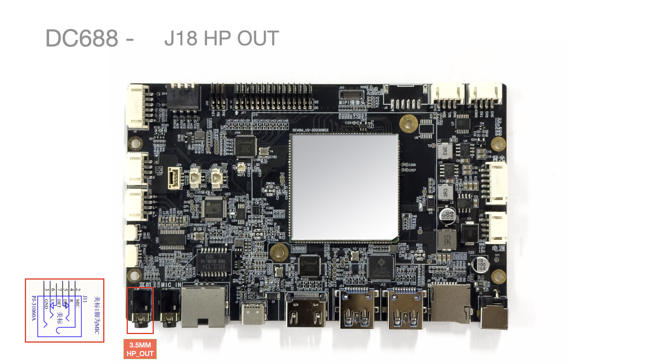
3.5MM interface: American standard (CTIA)
J18 3.5MM Microphone Interface
3.5MM interface: shared in parallel with MIC2
J20 Speaker/Power Amplifier Output
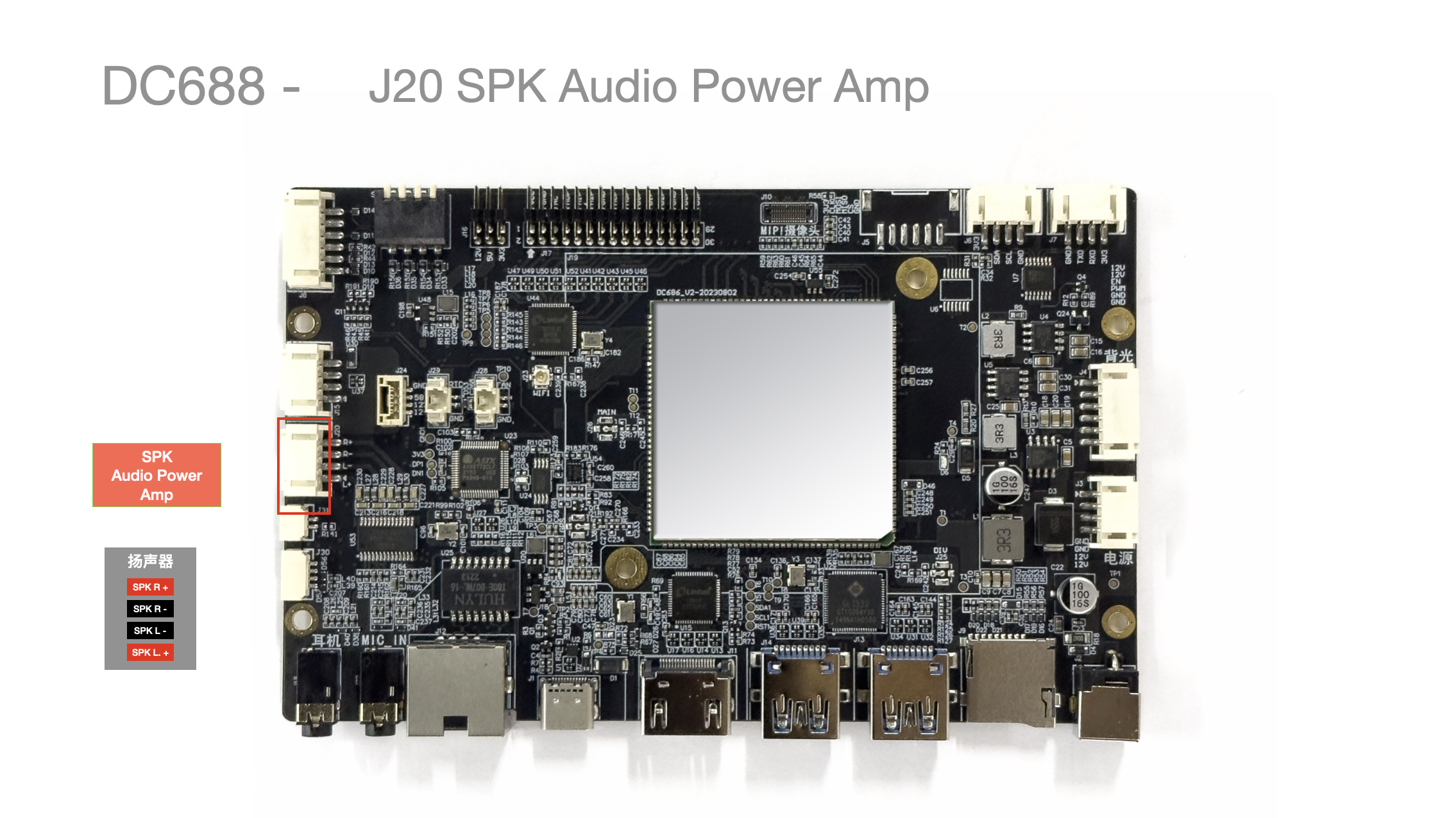
| Pin No. | Pin Description | Wire Color (Reference) |
|---|---|---|
| 1 | RP | Red |
| 2 | RN | Black |
| 3 | LN | Black |
| 4 | LP | Red |
J21/J23/J25/J26 WI-FI / BT/4G Antenna(s)
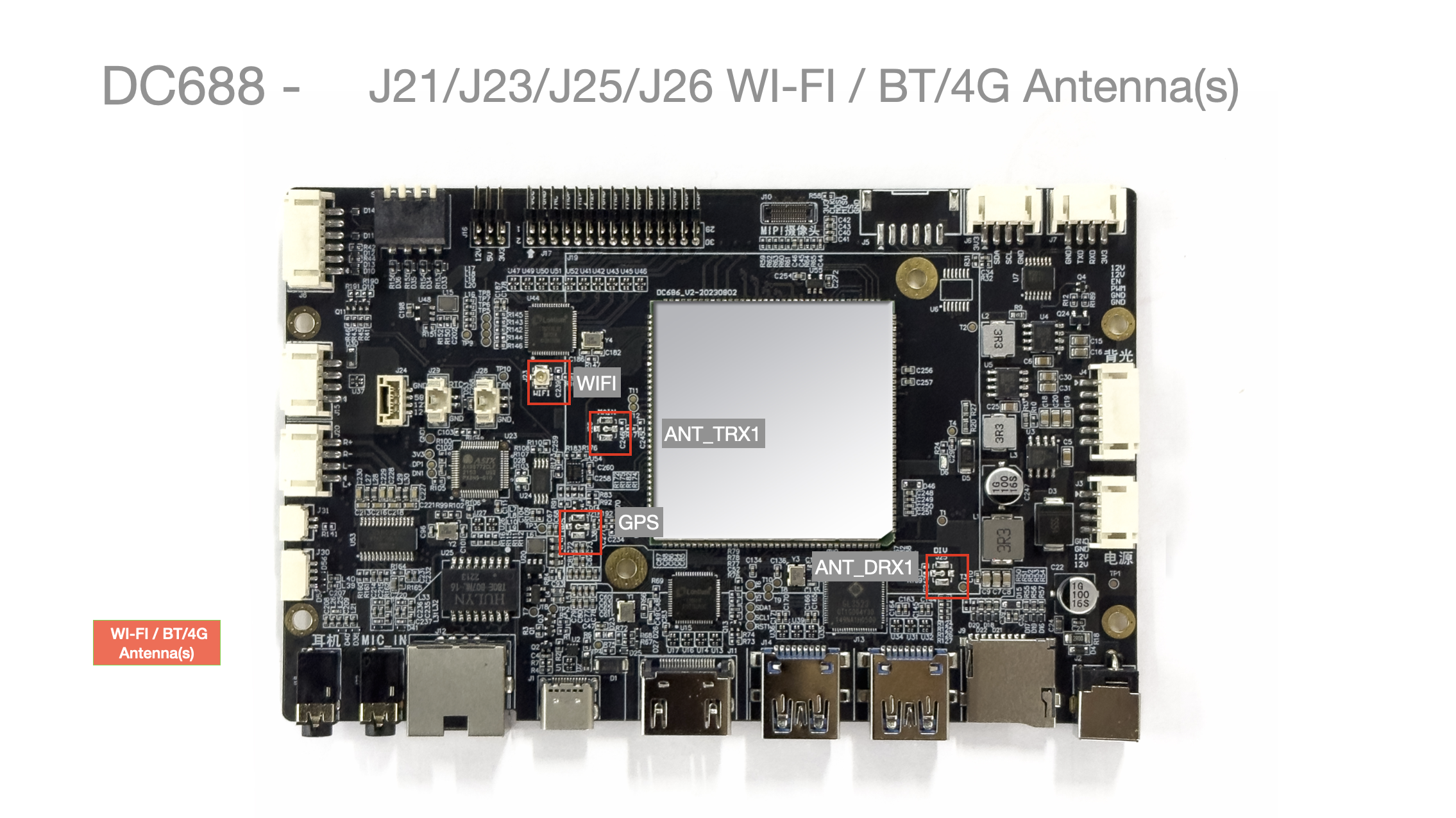
- For the standard version, only the J23 WI-FI antenna needs to be connected
J22 MIC 3.5MM Microphone Input
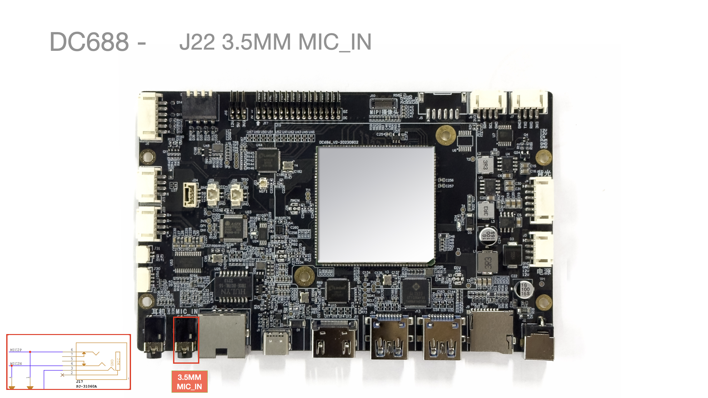
- American standard interface
J24 GPIO
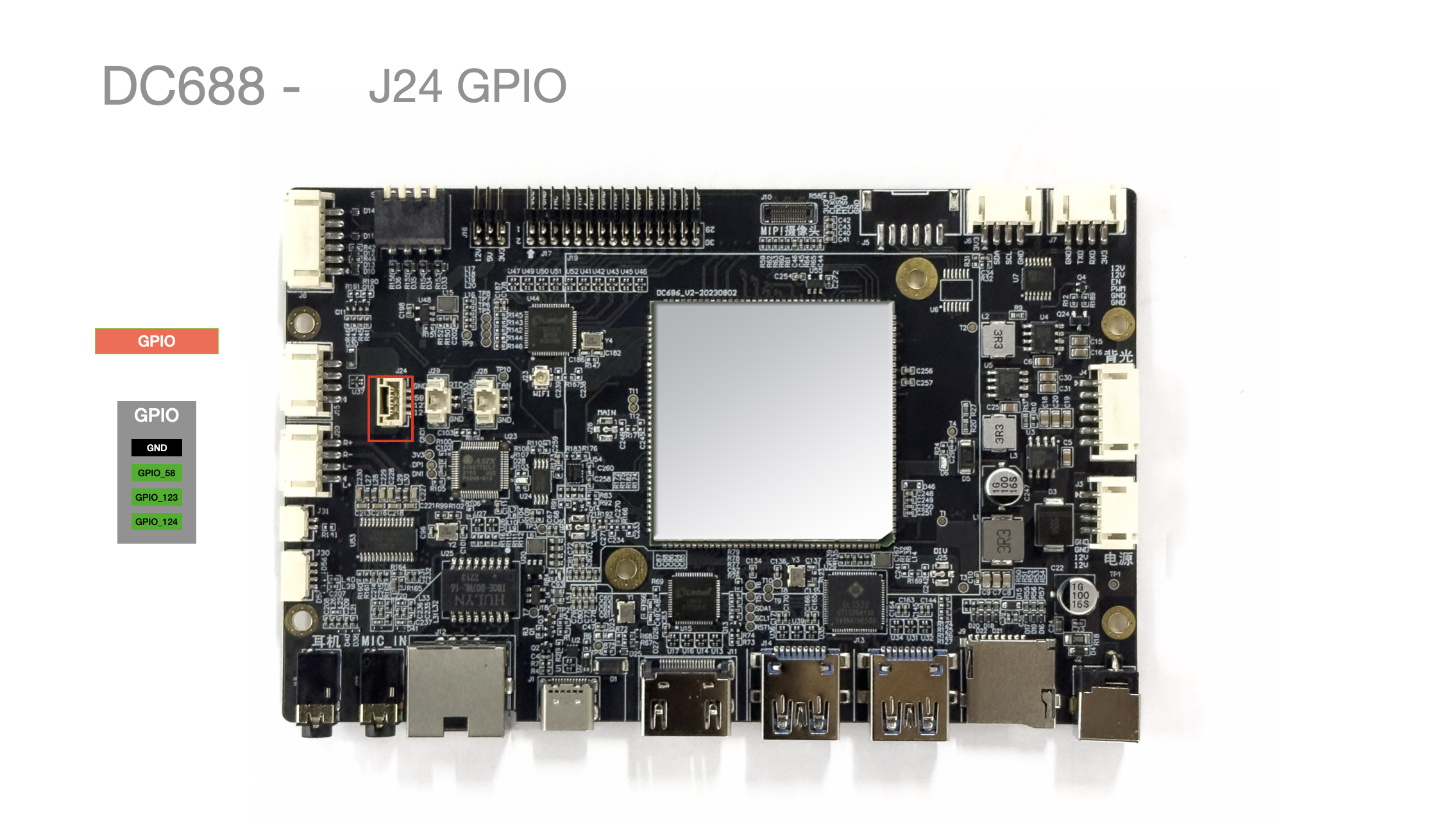
| Pin No. | Pin Description | Remarks |
|---|---|---|
| 1 | GPIO124 | 3v3 |
| 2 | GPIO123 | 3v3 |
| 3 | GPIO58 | 3v3 |
| 4 | GND | Ground |
J27 SIM-CARD Slot
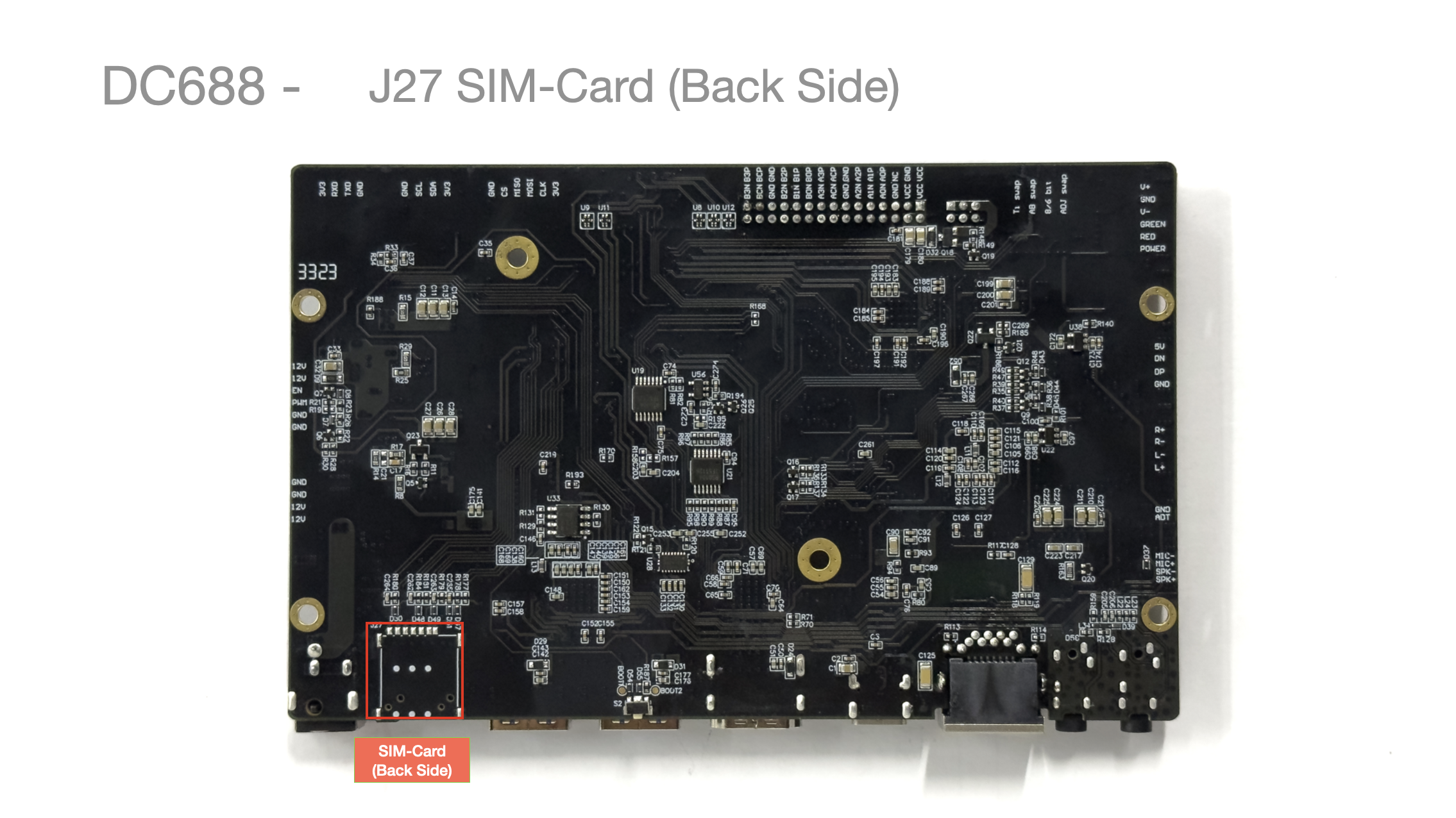
- Only installed on 4G versions
J28 SYS FAN Cooling Fan
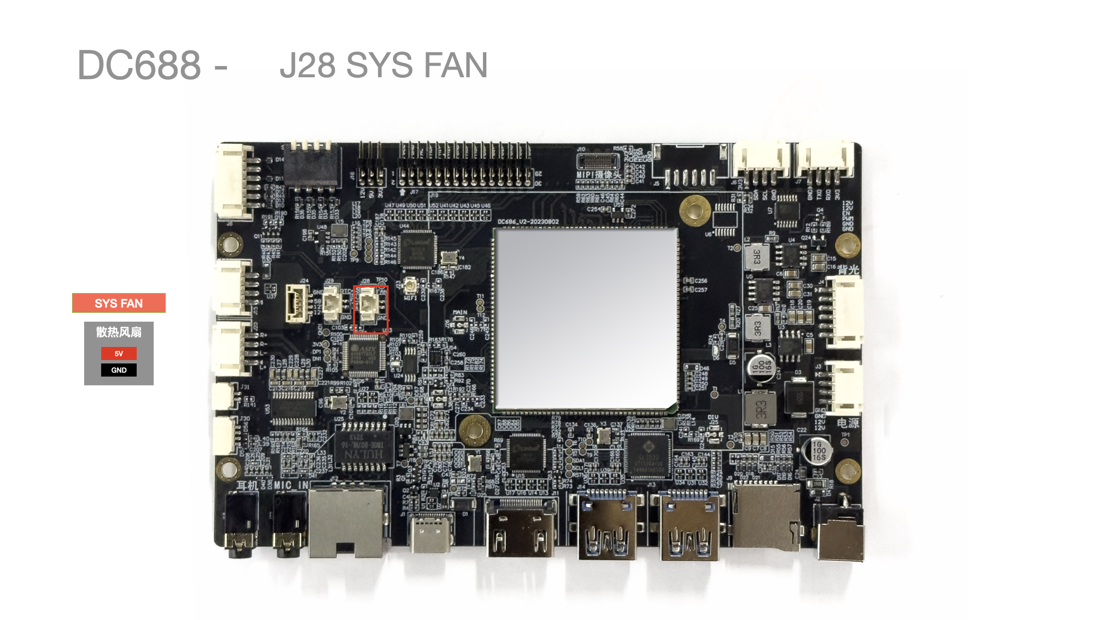
| Pin No. | Pin Description | Wire Color (Reference) |
|---|---|---|
| 1 | 5V | Red |
| 2 | GND | Black |
J29 RTC Battery
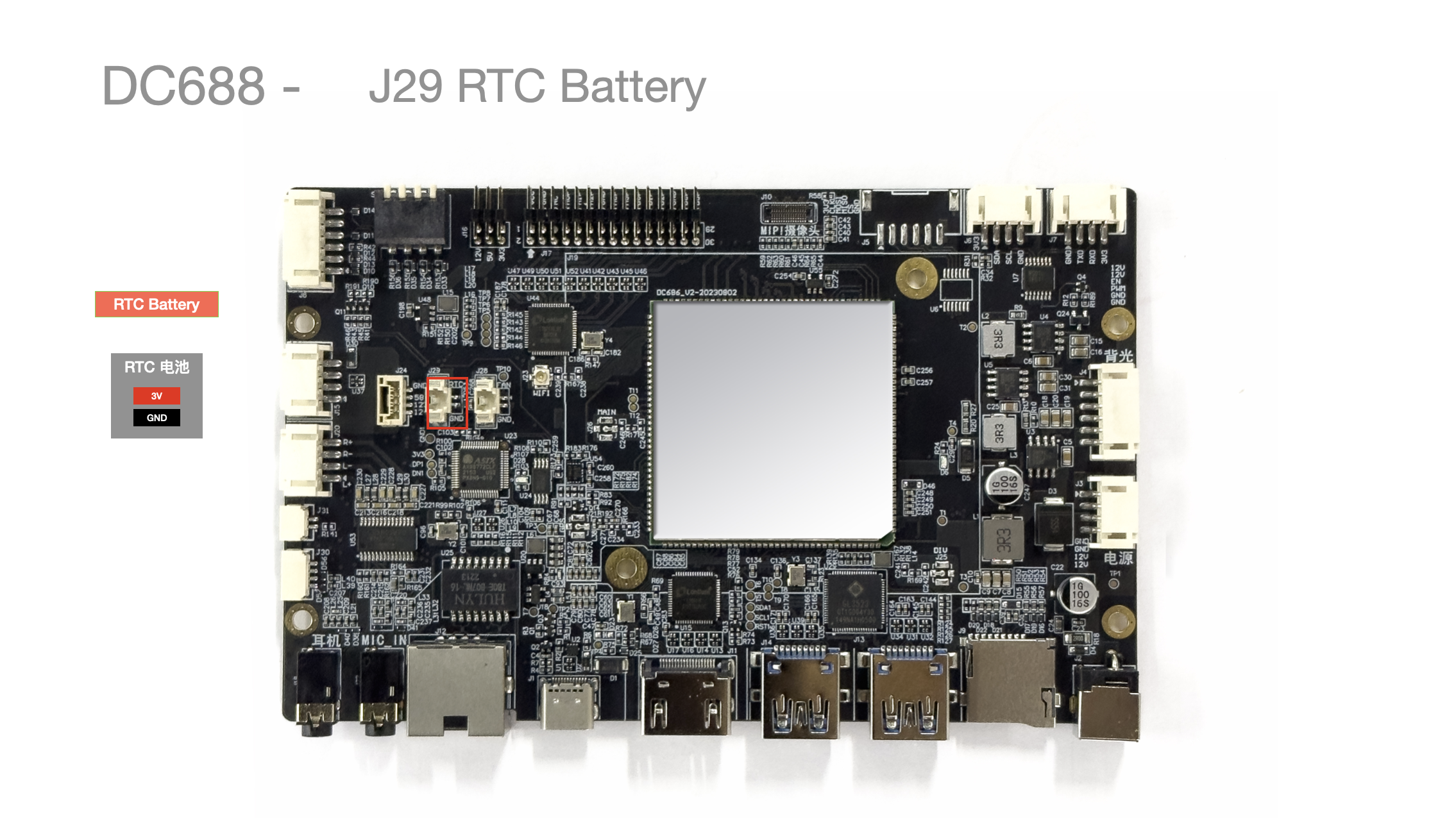
| Pin No. | Pin Description | Wire Color (Reference) |
|---|---|---|
| 1 | 3V3 | Red |
| 2 | GND | Black |
J30 MIC_IN/HPH_R
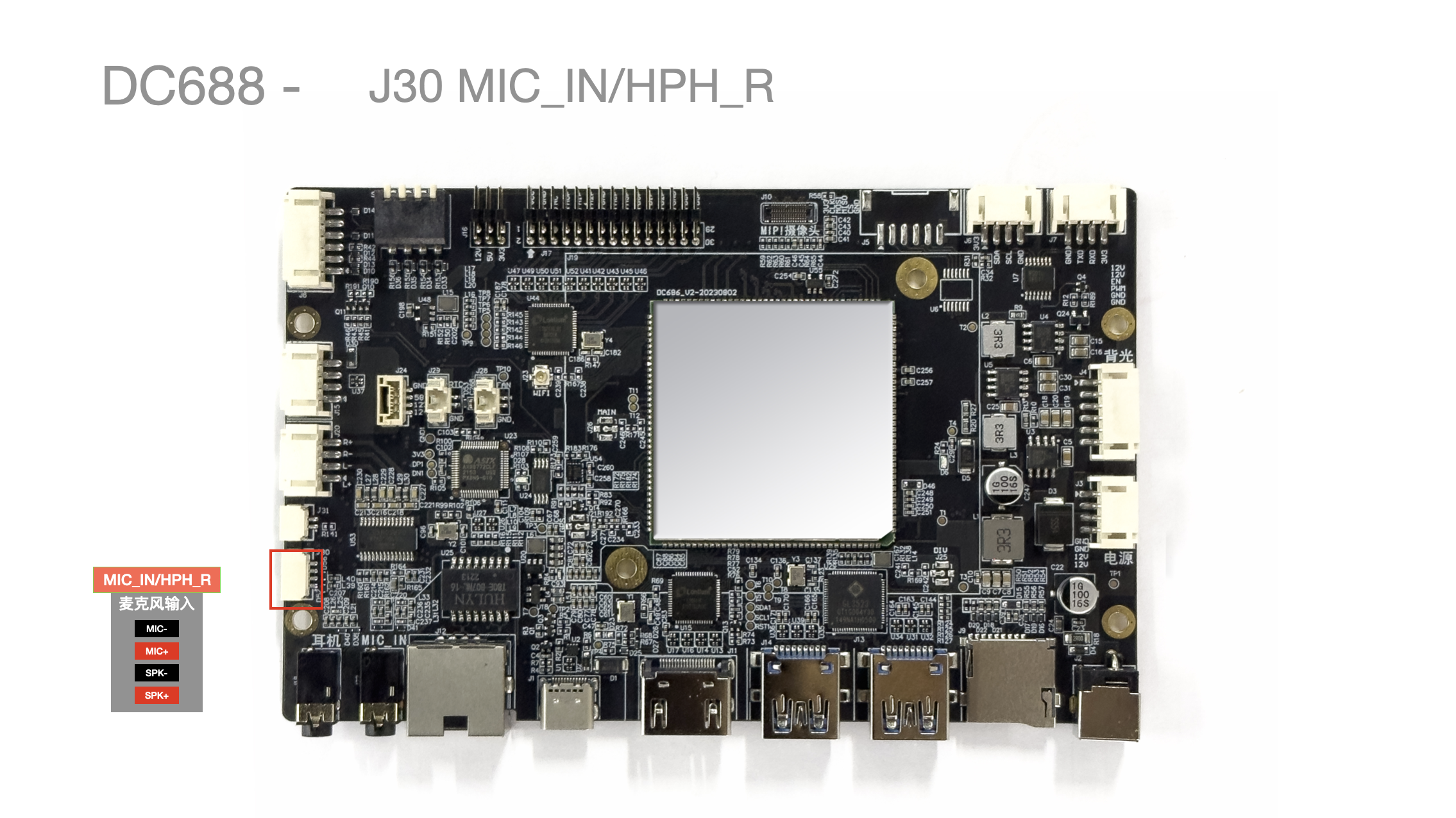
- Microphone input (MIC_IN) / right channel headphone output (HPH_R)
| Pin No. | Pin Description | Remarks |
|---|---|---|
| 1 | CDC_HPH_R | |
| 2 | CDC_HPH_REF | |
| 3 | MIC2_P | |
| 4 | MIC2_N |
J31 MBHC_HSDET
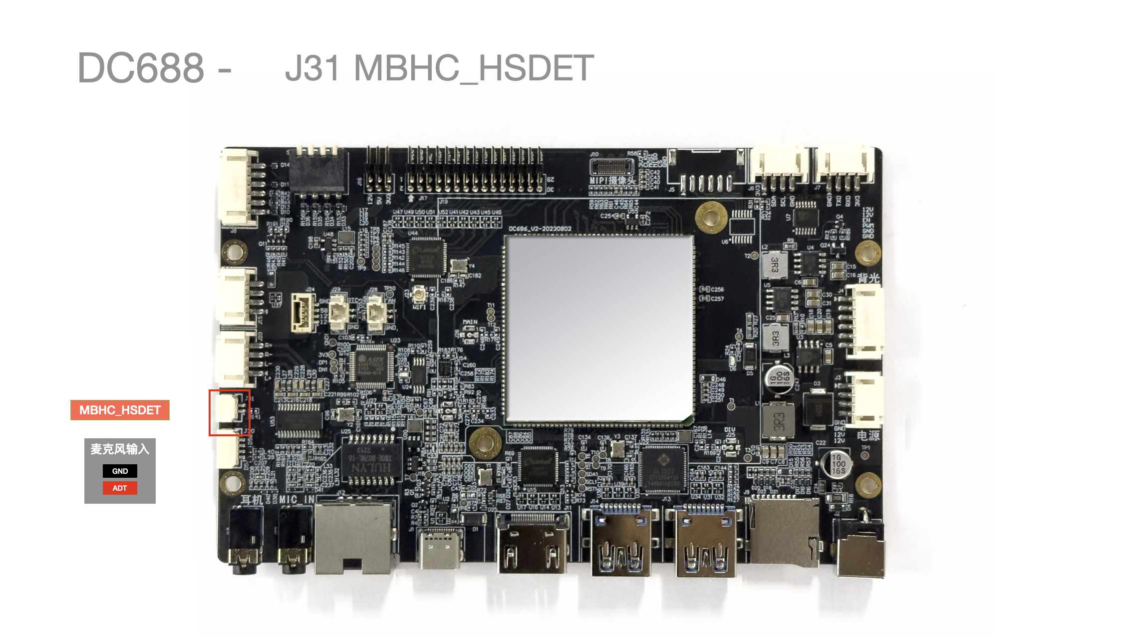
- Microphone input detection (MBHC_HSDET)
| Pin No. | Pin Description | Remarks |
|---|---|---|
| 1 | MBHC_HSDET_L | |
| 2 | GND |
S1 DIP Switch
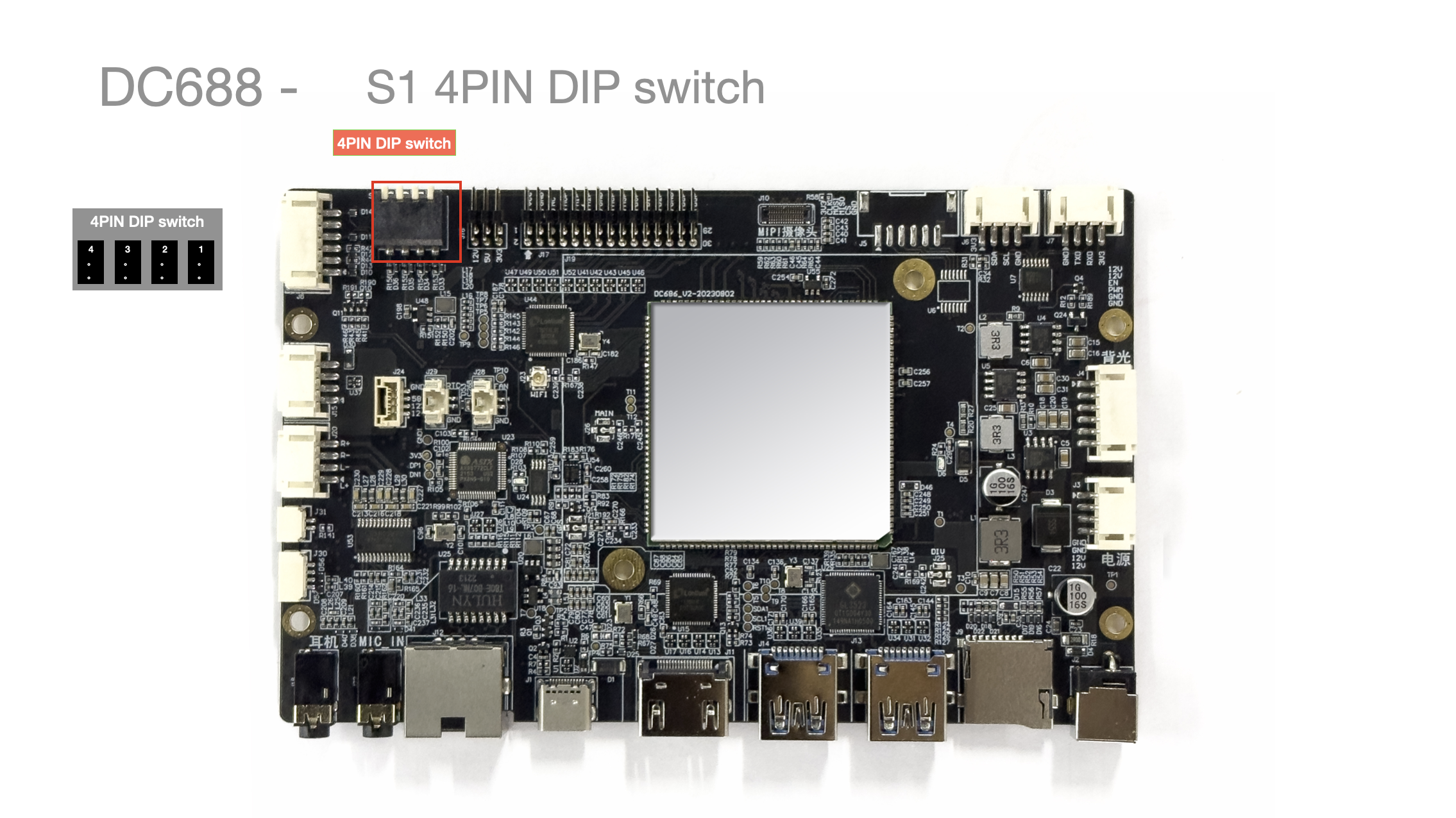
- Part model:
DSPV04LSGET, DIP Switch-Side Piano Key-SMD-2.54mm-4 Position-DSPV04LSGET
DIP No. Name State (Up/Down) Corresponding Function Remarks 1 TAG_DATA_FORMAT Up/Pressed JEIDA Abnormal screen colors 2 TAG_PORT_WASP Up/Pressed 1 Stripes on the screen 3 TAG_COLOR_DEPTH Up/Pressed DEPTH_6BIT Color cast on the screen 4 Backlight polarity adjustment Up/Pressed Polarity reversed Brightness decreases when increased
Pressing toward the PCB means
S2 Boot Upgrade Button
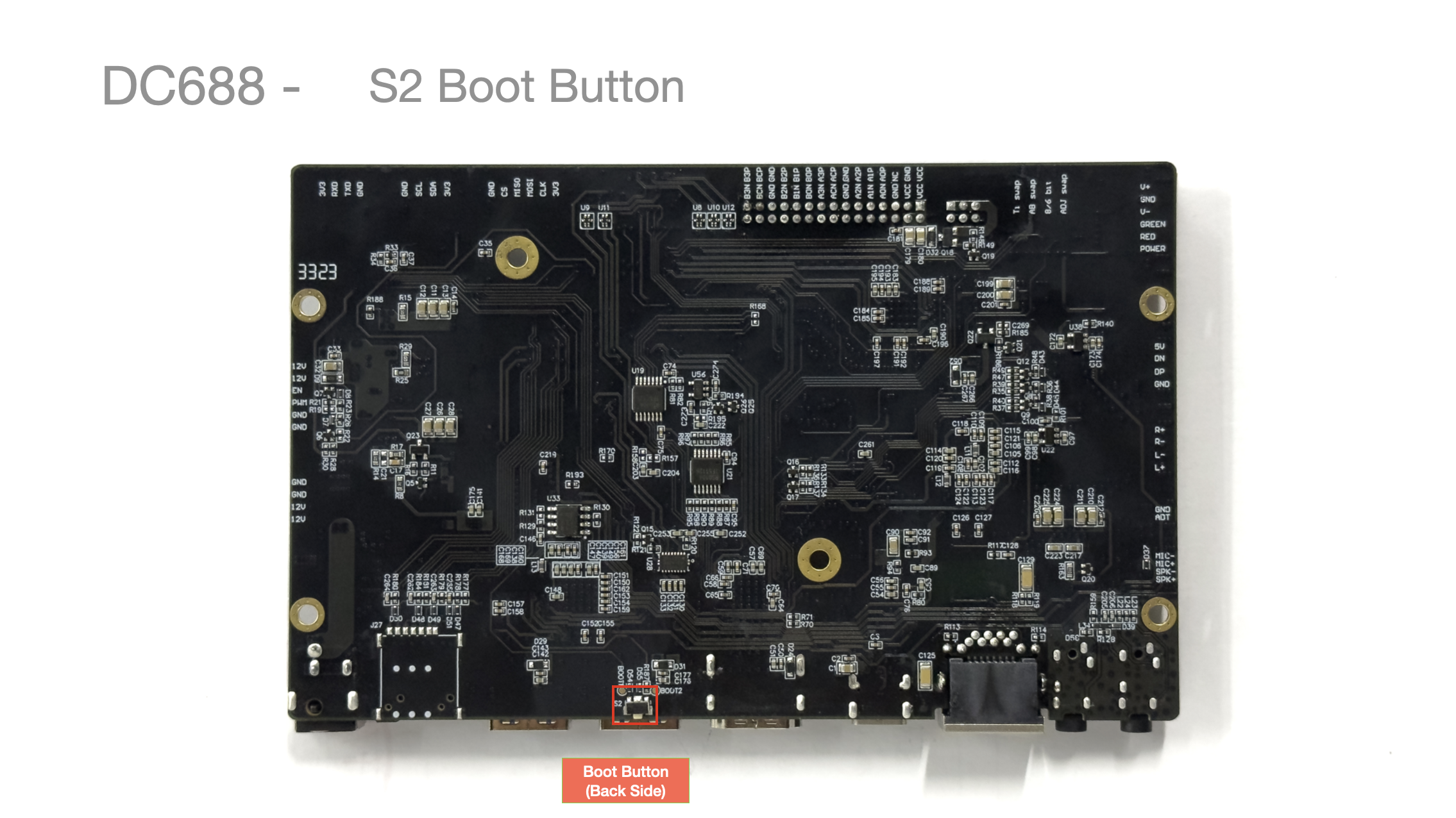
Press and hold while powering on / applying power to enter