Interface Definitions

The IM2290 provides a rich set of interfaces, as shown in the following diagram:
/dc2290/DC2290 /im2290/IM2290
Overall Interface Diagram
Overall Device Interfaces
J1 Relay/USB/Network Port/Power Supply
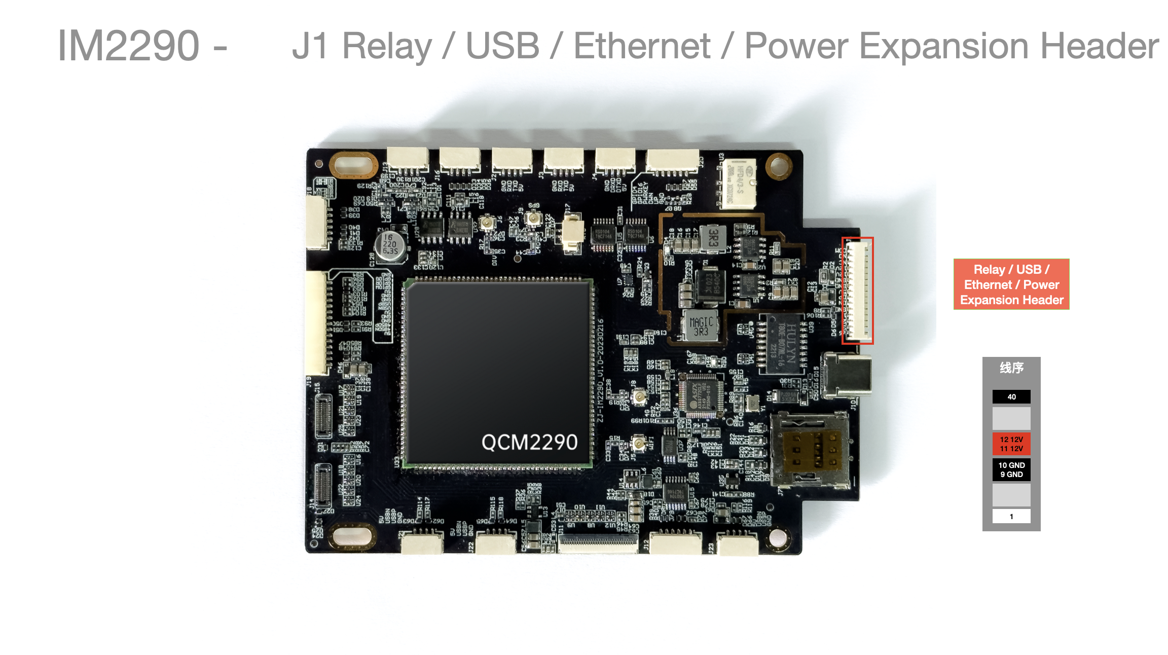
| Pin No. | Device Name | Notes |
|---|---|---|
| 1 | T_TB_N | Ethernet T_TB_N : 6 |
| 2 | T_TB_P | Ethernet T_TB_P : 3 |
| 3 | T_TA_N | Ethernet T_TA_N : 2 |
| 4 | T_TA_P | Ethernet T_TA_P : 1 |
| 5 | GND | USB |
| 6 | USB2_DN | USB |
| 7 | USB2_DP | USB |
| 8 | 5V | USB |
| 9 | GND | Power Supply |
| 10 | GND | Power Supply |
| 11 | 12V | Power Supply |
| 12 | 12V | Power Supply |
| 13 | NC | Relay NC: Normally Closed |
| 14 | NO | Relay NO: Normally Open |
| 15 | COM | Relay COM: GPIO31 |
J2, J3, J4 Serial Ports
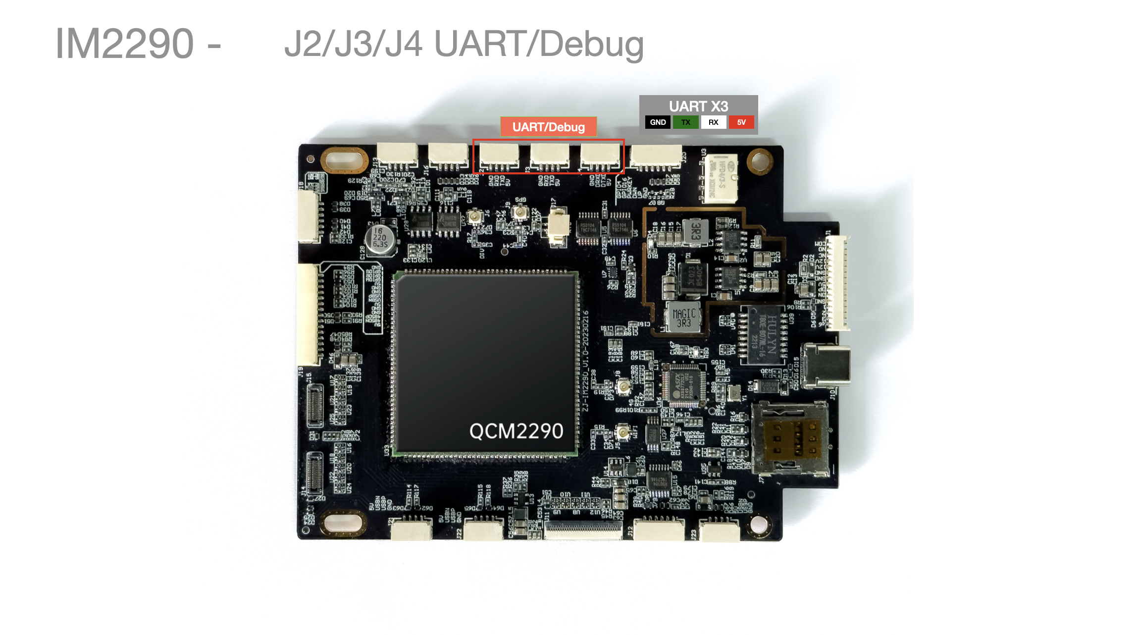
| Pin No. | Device Name | Notes |
|---|---|---|
| J2 1 | GND | ttyHS1 |
| J2 2 | RXD | ttyHS1 |
| J2 3 | TXD | ttyHS1 |
| J2 4 | 5V | ttyHS1 |
| J3 1 | GND | ttyHS2 |
| J3 2 | RXD | ttyHS2 |
| J3 3 | TXD | ttyHS2 |
| J3 4 | 5V | ttyHS2 |
| J4 1 | GND | ttyHS3 Original Debug UART Interface |
| J4 2 | RXD | ttyHS3 Original Debug UART Interface |
| J4 3 | TXD | ttyHS3 Original Debug UART Interface |
| J4 4 | 5V | ttyHS3 Original Debug UART Interface |
J5, J6, J8, J9 Antenna Interfaces
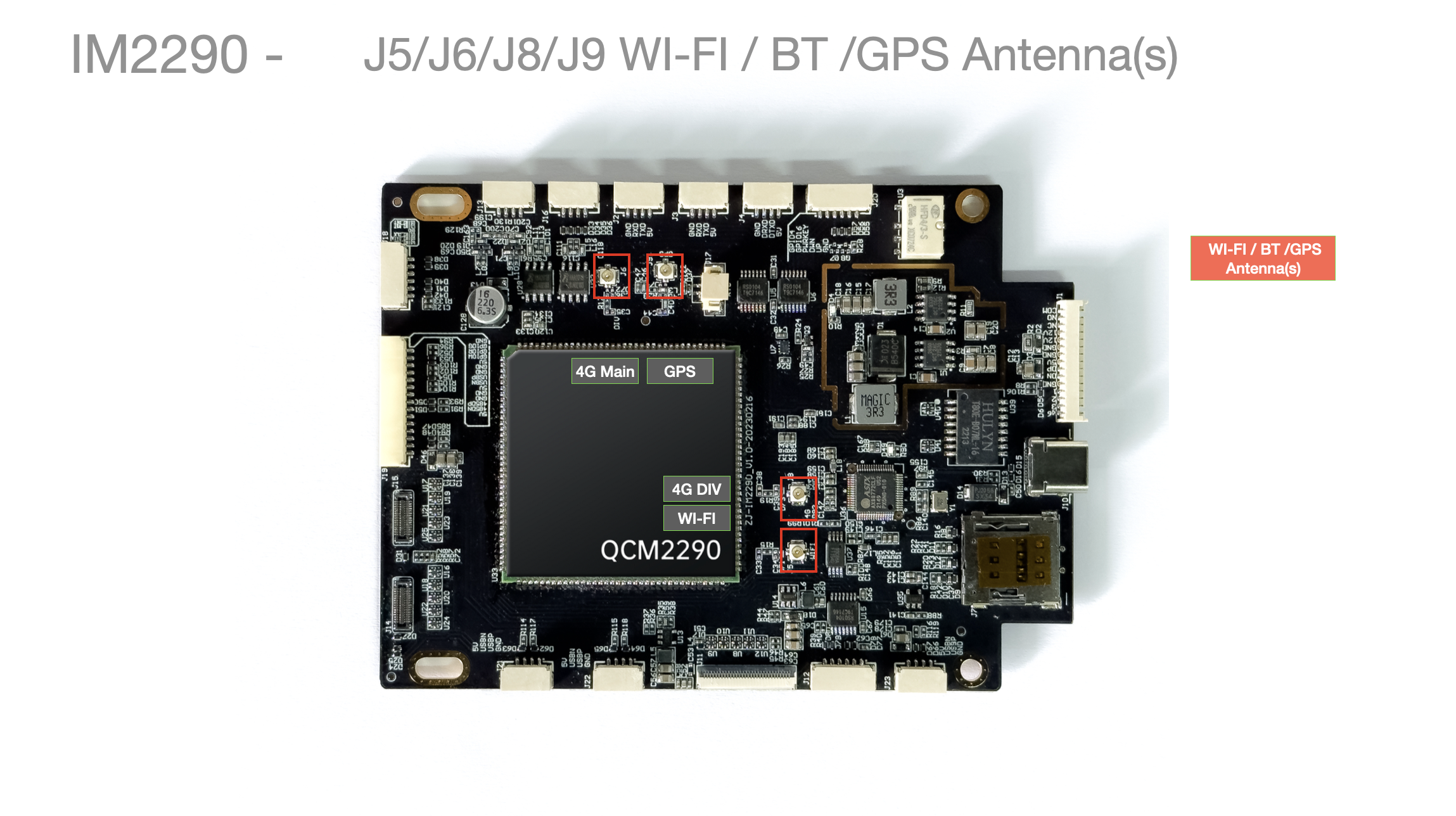
| Pin No. | Device Name | Notes |
|---|---|---|
| J5 | WIFI Antenna Connector | |
| J6 | 4G Diversity Antenna Connector | |
| J8 | 4G Main Antenna Connector | |
| J9 | GPS Antenna Connector |
J7 Nano SIM Card Slot
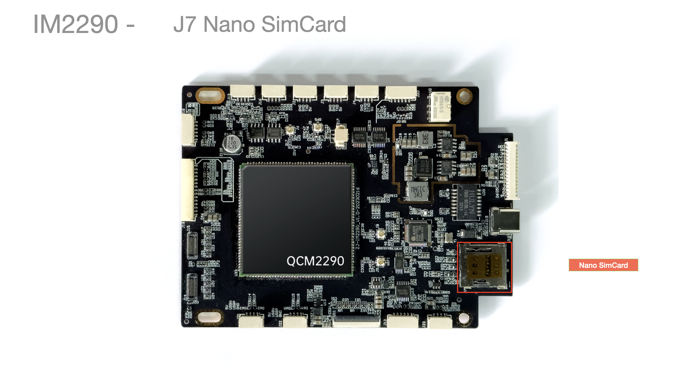
- Nano SIM card slot
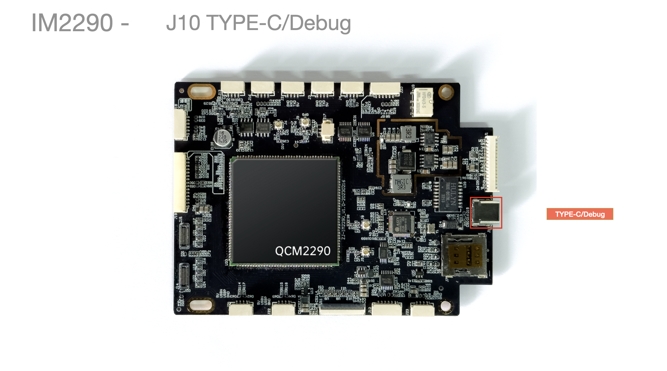
J10 type-C Interface
-
The IM2290 control board provides a TYPE-C interface for module system firmware upgrade.
-
Note: Powering via type-C will cause the hub chip to stop working, and the USB interfaces will become non-functional.
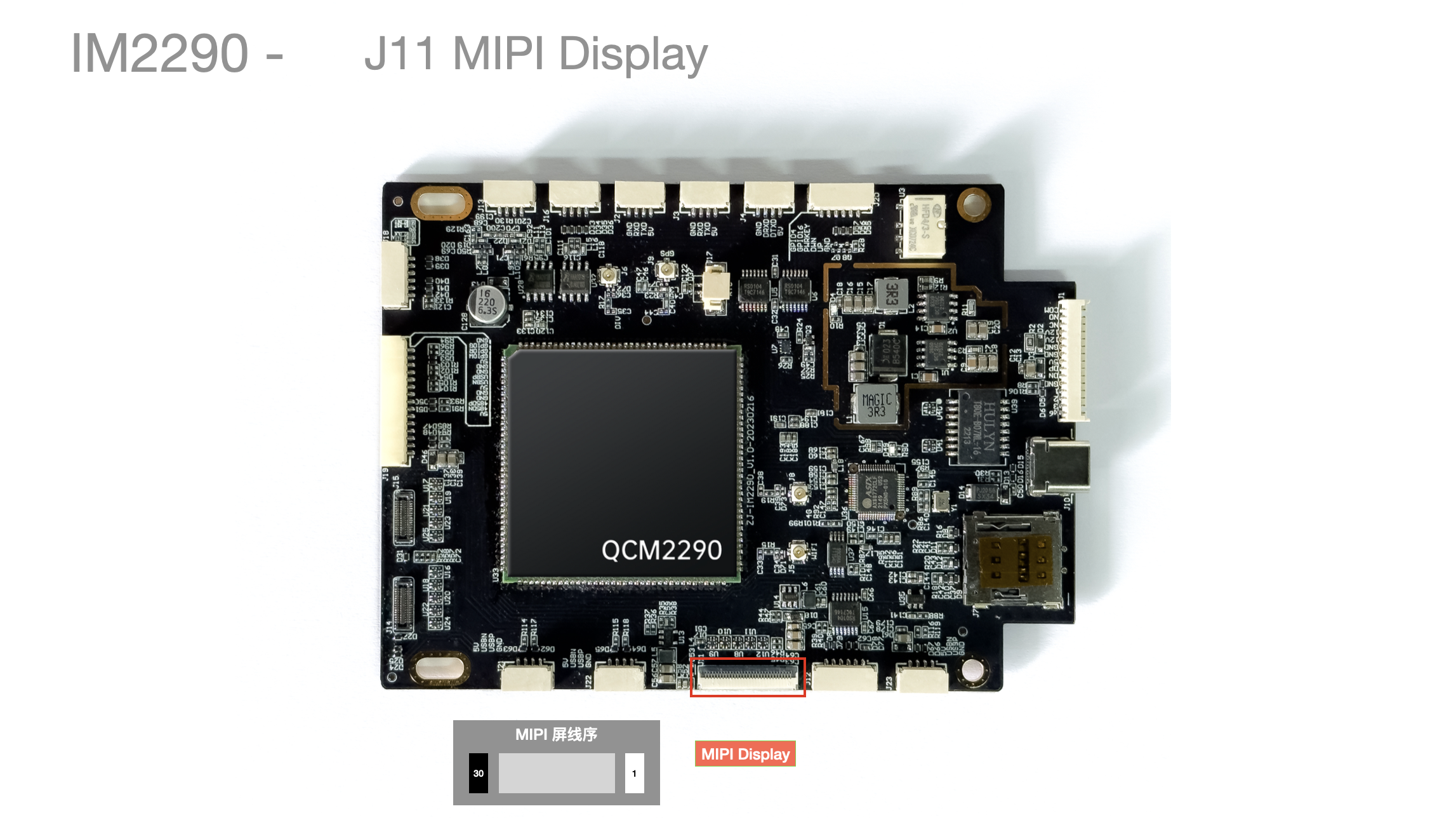
J11 MIPI Main Screen Interface
J12 TP Touch Interface
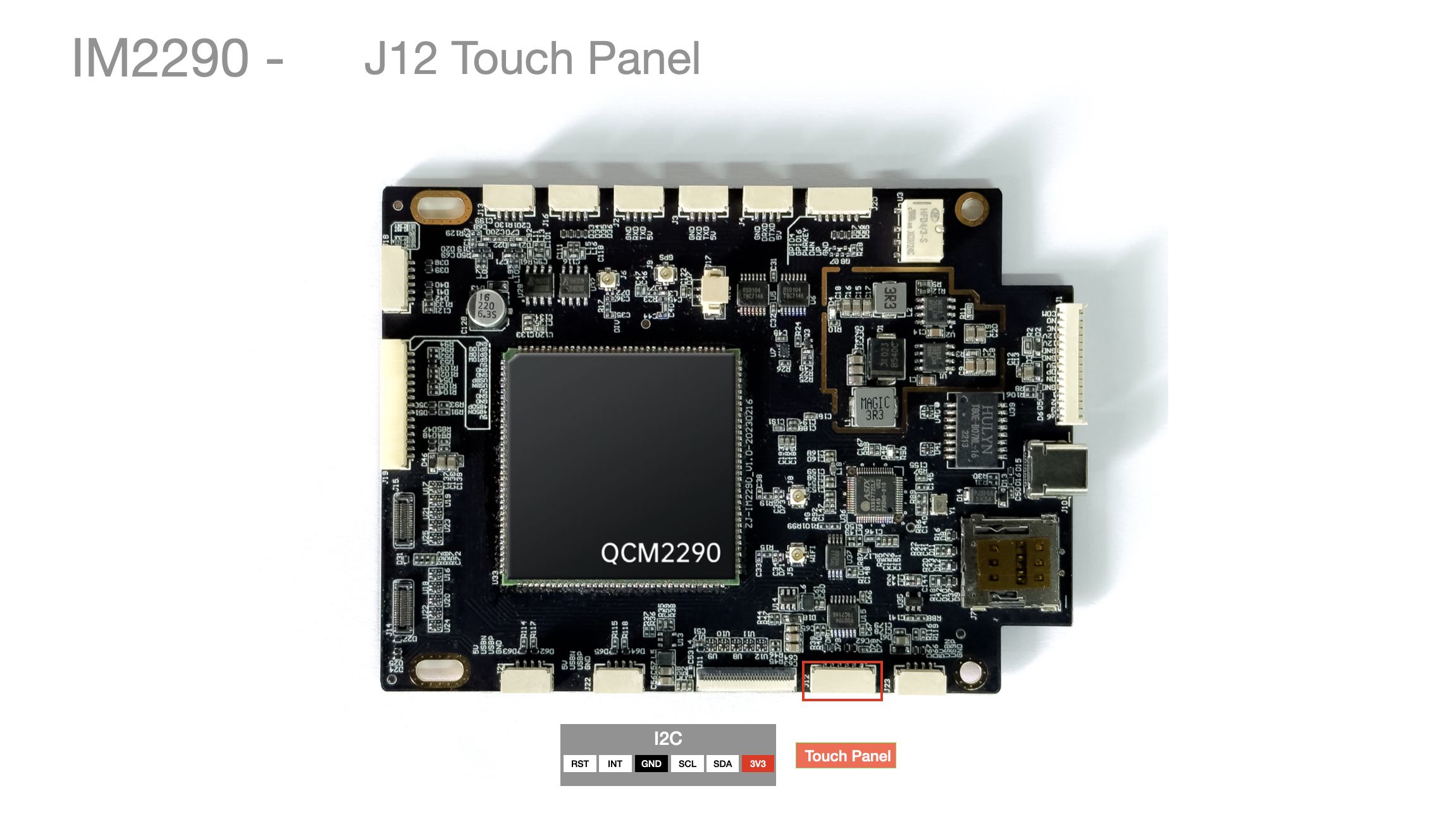
| Pin No. | Device Name | Notes |
|---|---|---|
| 1 | 3V3_TP | |
| 2 | TP_SDA | |
| 3 | TP_SCL | |
| 4 | GND | |
| 5 | TP_INT1 | |
| 6 | TP_RST |
J13 MIC Interface
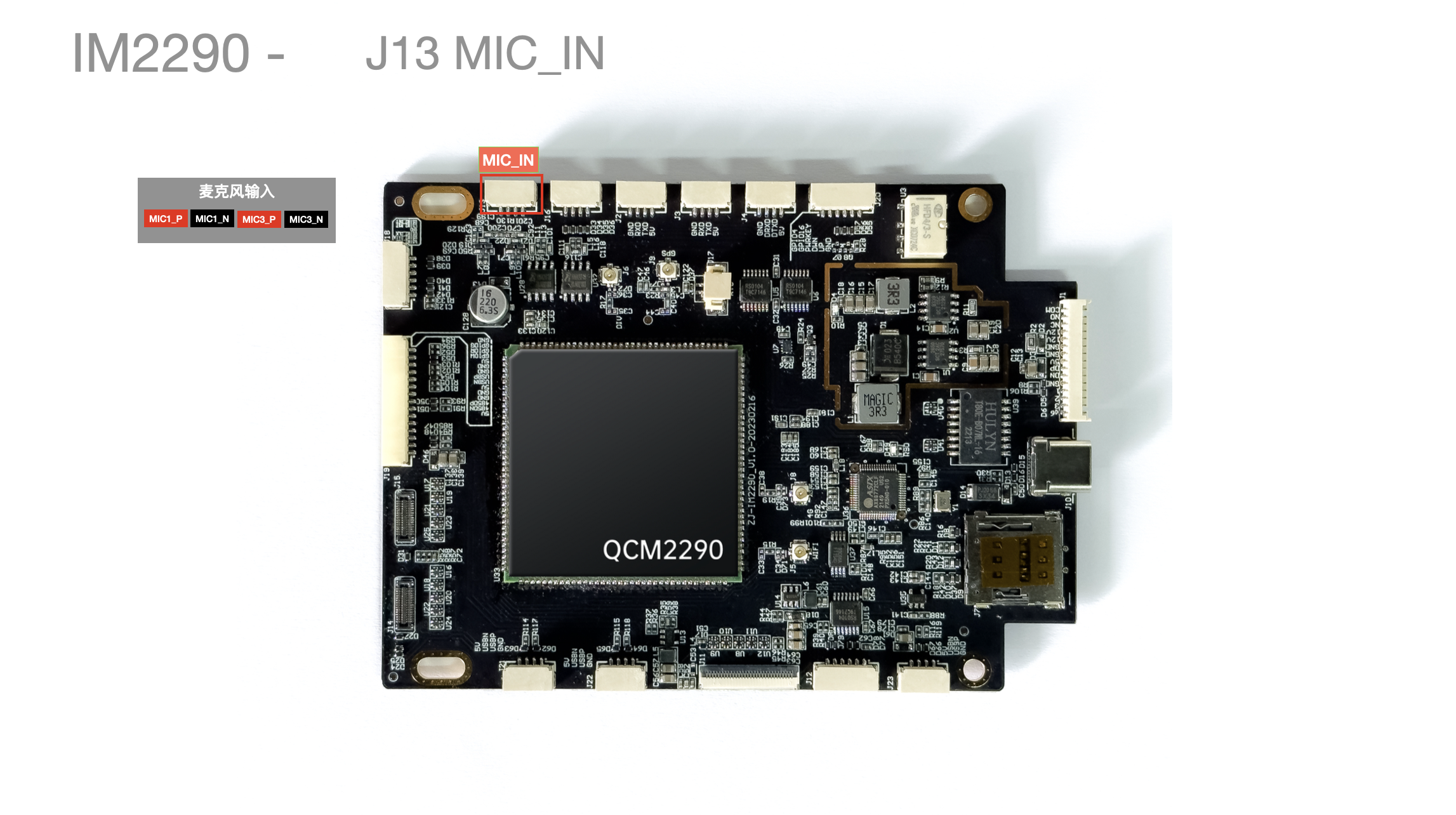
| Pin No. | Device Name | Notes |
|---|---|---|
| 1 | MIC1_P | |
| 2 | MIC1_N | |
| 3 | MIC3_P | |
| 4 | MIC3_N |
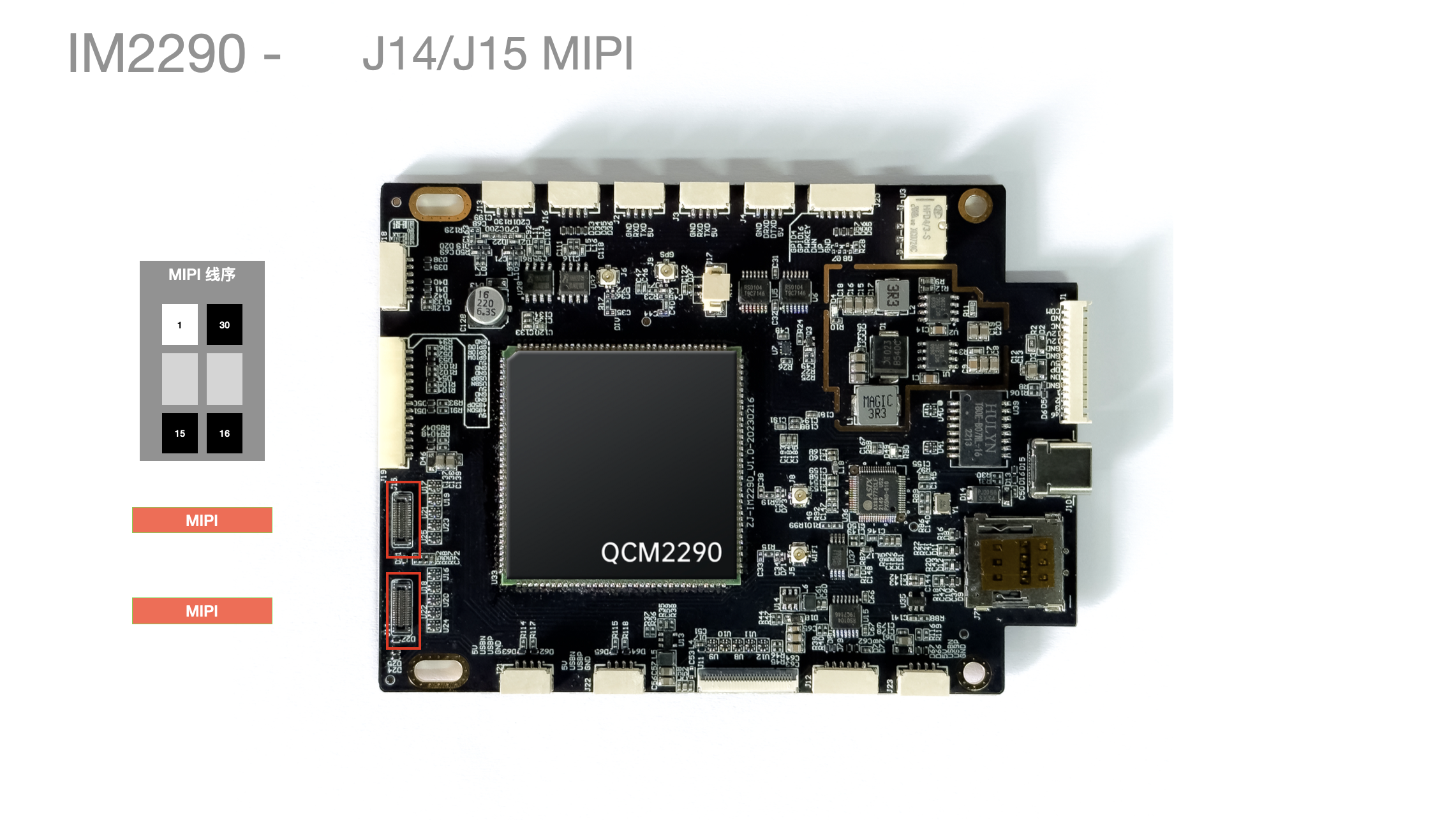
J14, J15 MIPI Cameras
J16 Speaker
4 Ohm 3W
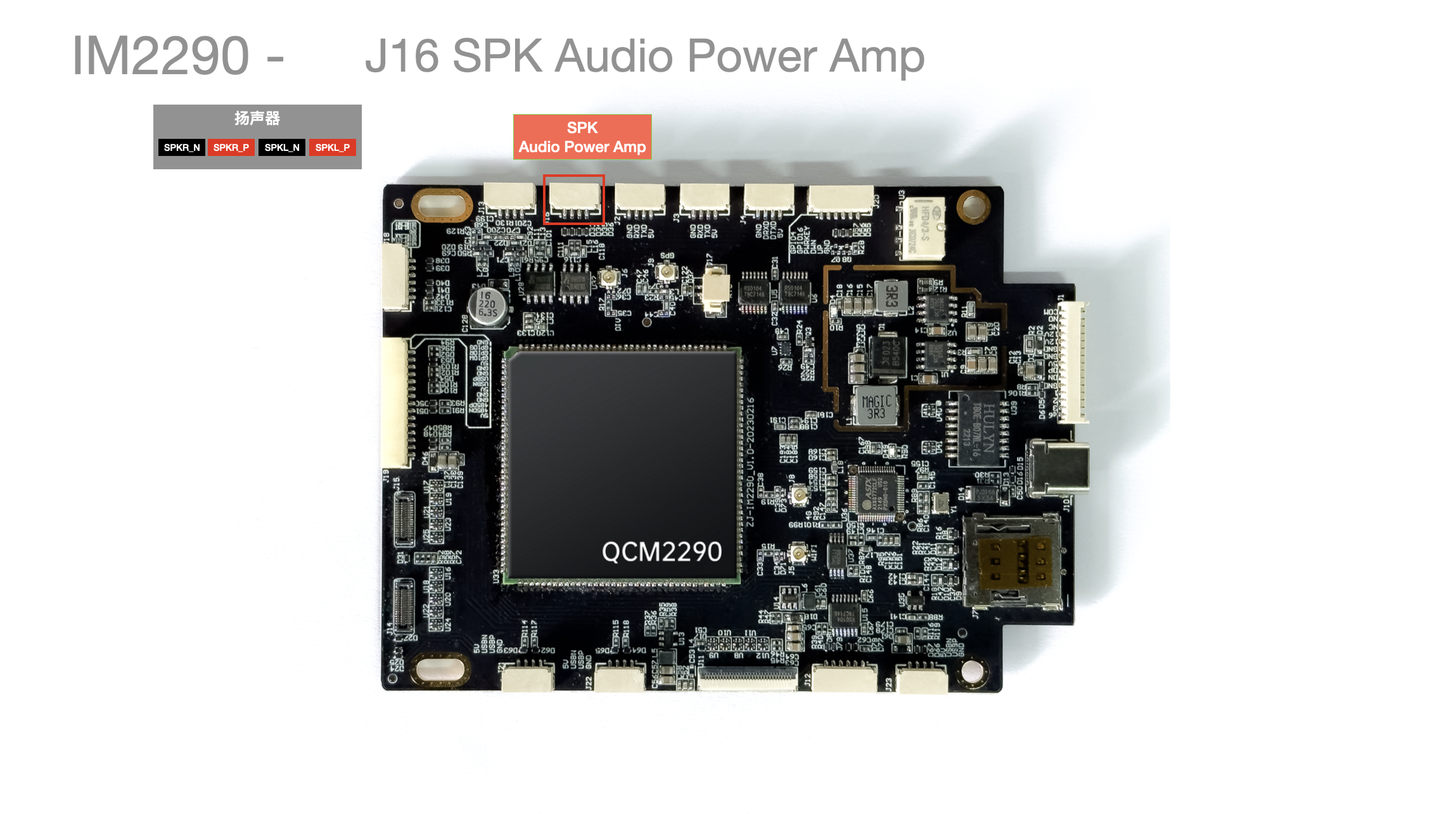
| Pin No. | Device Name | Notes |
|---|---|---|
| 1 | SPKRN | Right Channel |
| 2 | SPKRP | Right Channel |
| 3 | SPKLN | Left Channel |
| 4 | SPKLP | Left Channel |
J17 RTC Battery
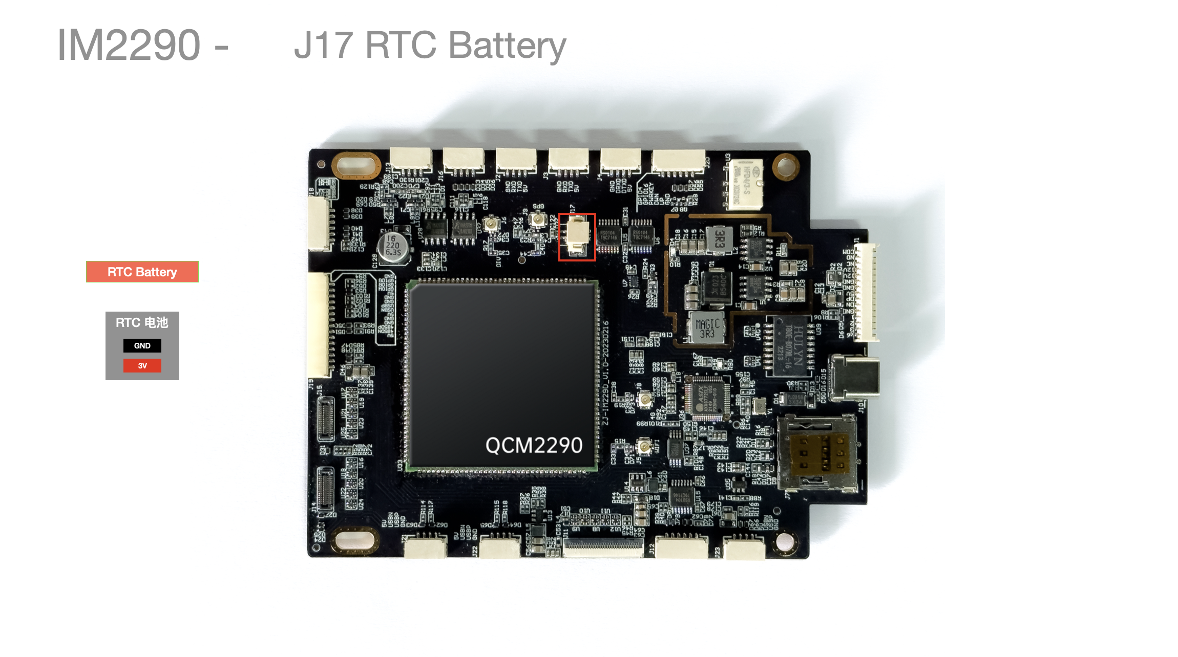
| Pin No. | Device Name | Notes |
|---|---|---|
| 1 | RTC | 3V |
| 2 | GND |
J18 SIM Card Expansion
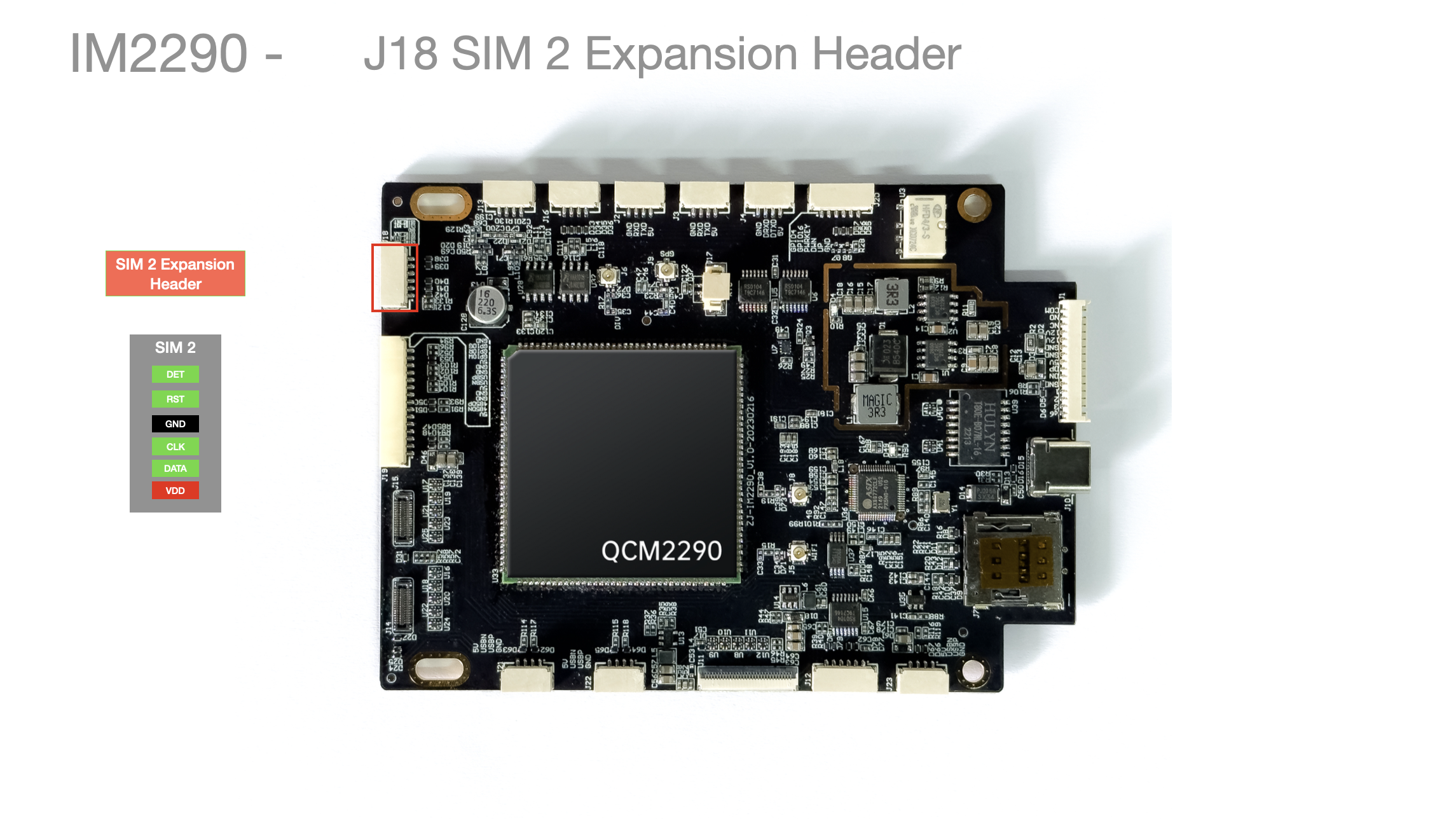
| Pin No. | Pin Description | Notes |
|---|---|---|
| 1 | USIM2_VDD | |
| 2 | USIM2_DATA | |
| 3 | USIM2_CLK | |
| 4 | GND | |
| 5 | USIM2_RST | |
| 6 | USIM2_DET |
J19 USB*2/GPIO
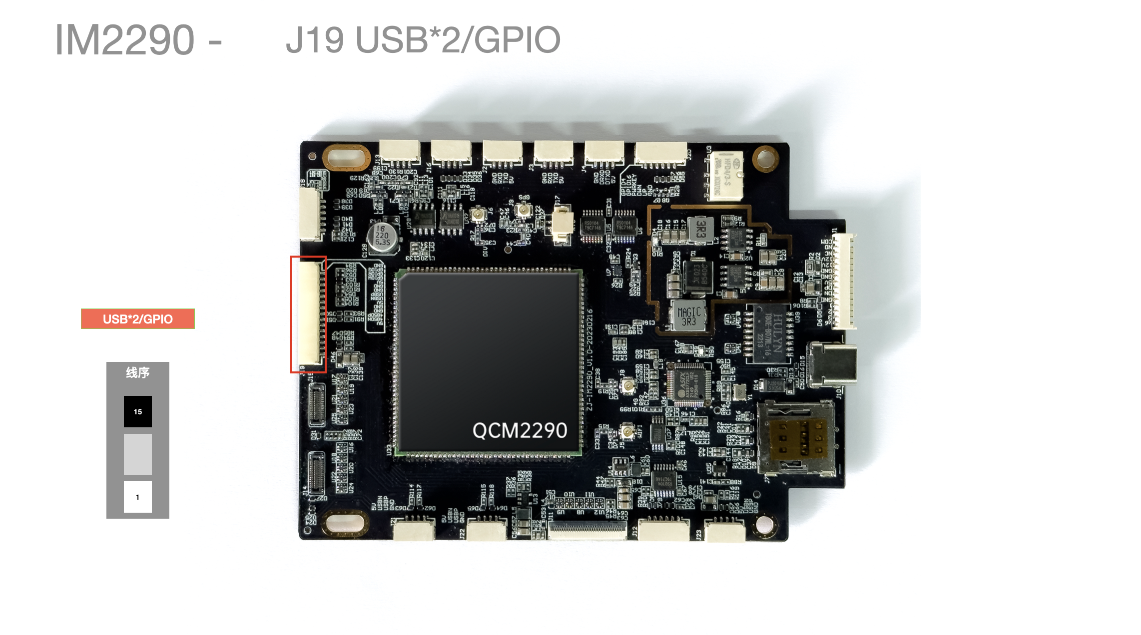
| Pin No. | Device Name | Notes |
|---|---|---|
| 1 | 5V_CAMRA | USB1 for camera connection |
| 2 | USBA4_N | USB1 for camera connection |
| 3 | USBA4_P | USB1 for camera connection |
| 4 | GND | USB1 for camera connection |
| 5 | GND | USB1 for camera connection |
| 6 | 5V_CAMRA | USB2 for camera connection |
| 7 | USBA3_N | USB2 for camera connection |
| 8 | USBA3_P | USB2 for camera connection |
| 9 | GND | USB2 for camera connection |
| 10 | GND | USB2 for camera connection |
| 11 | 5V_CAMRA | GPIO for LED strip connection |
| 12 | GPIO_W | GPIO_W:GPIO107 |
| 13 | GPIO_R | GPIO_R:GPIO32 |
| 14 | GPIO_G | GPIO_G:GPIO56 |
| 15 | GND | GPIO for LED strip connection |
J20 Buttons
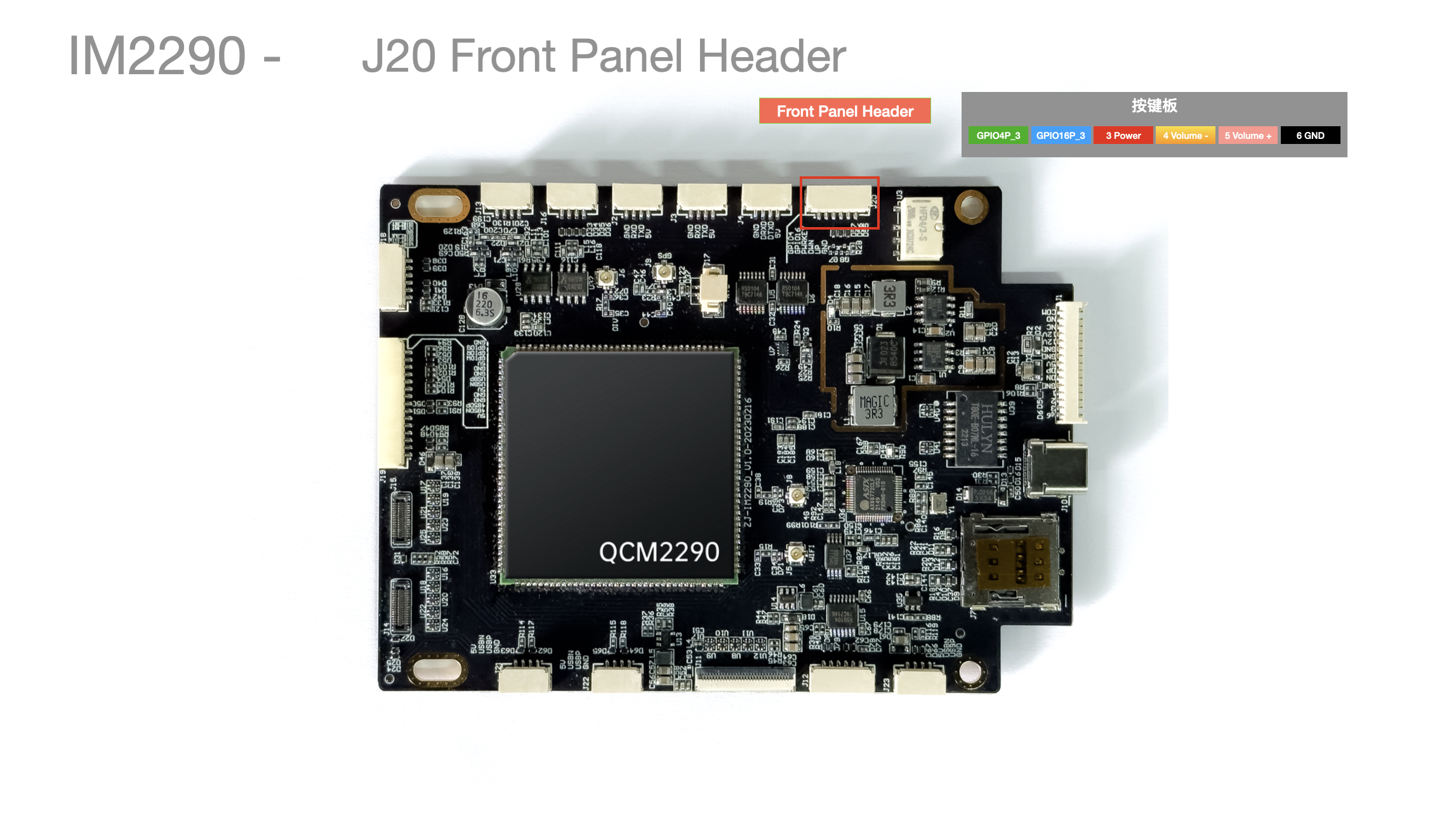
| Pin No. | Device Name | Notes |
|---|---|---|
| 1 | GPIO_4P_3 | |
| 2 | GPIO_16_3 | |
| 3 | PWRKEY | |
| 4 | KEY_VOL_DOWN | |
| 5 | KEY_VOL_UP | |
| 6 | GND |
J21/J22/J23 USB
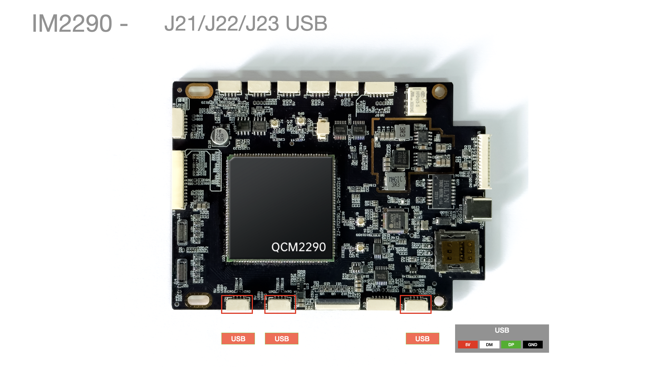
| Pin No. | Device Name | Notes |
|---|---|---|
| 1 | GND | |
| 2 | USBA5_P | |
| 3 | USBA5_N | |
| 4 | 5V |
S1 Boot Button
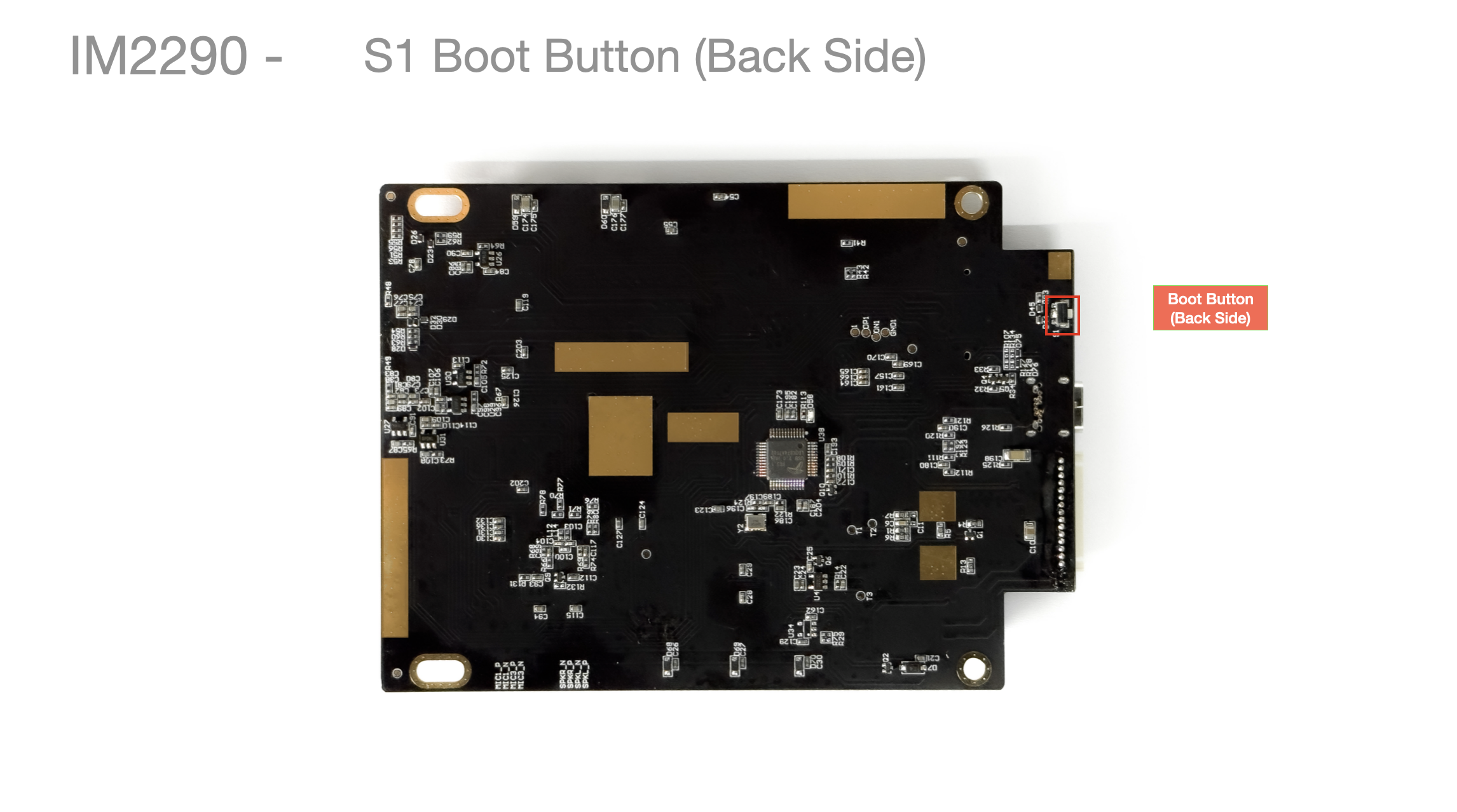
- Located below the J7 nano SIM card slot, used to enter burning mode.