Interface Definitions

DC685-G provides a rich set of interfaces, as shown below:
Device Interface Definitions
Device interfaces
J1 Buttons
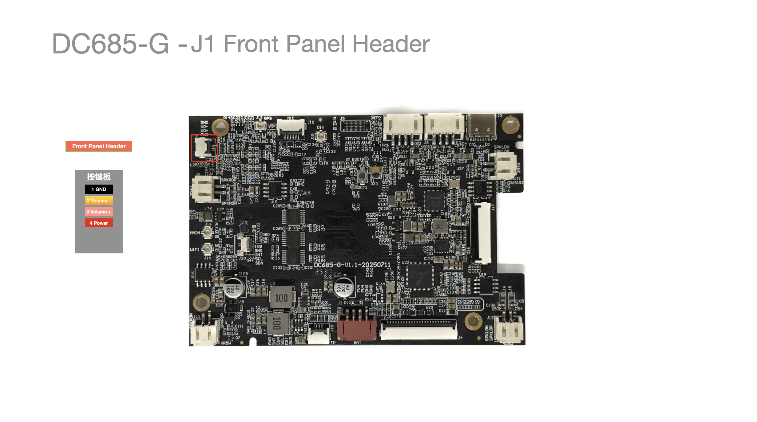
| Pin No. | Pin Description | Remarks |
|---|---|---|
| 1 | GND | Ground |
| 2 | VOL_DOWN_N | Volume - |
| 3 | VOL_UP_N | Volume + |
| 4 | POWK | Power button |
J2 Type-C
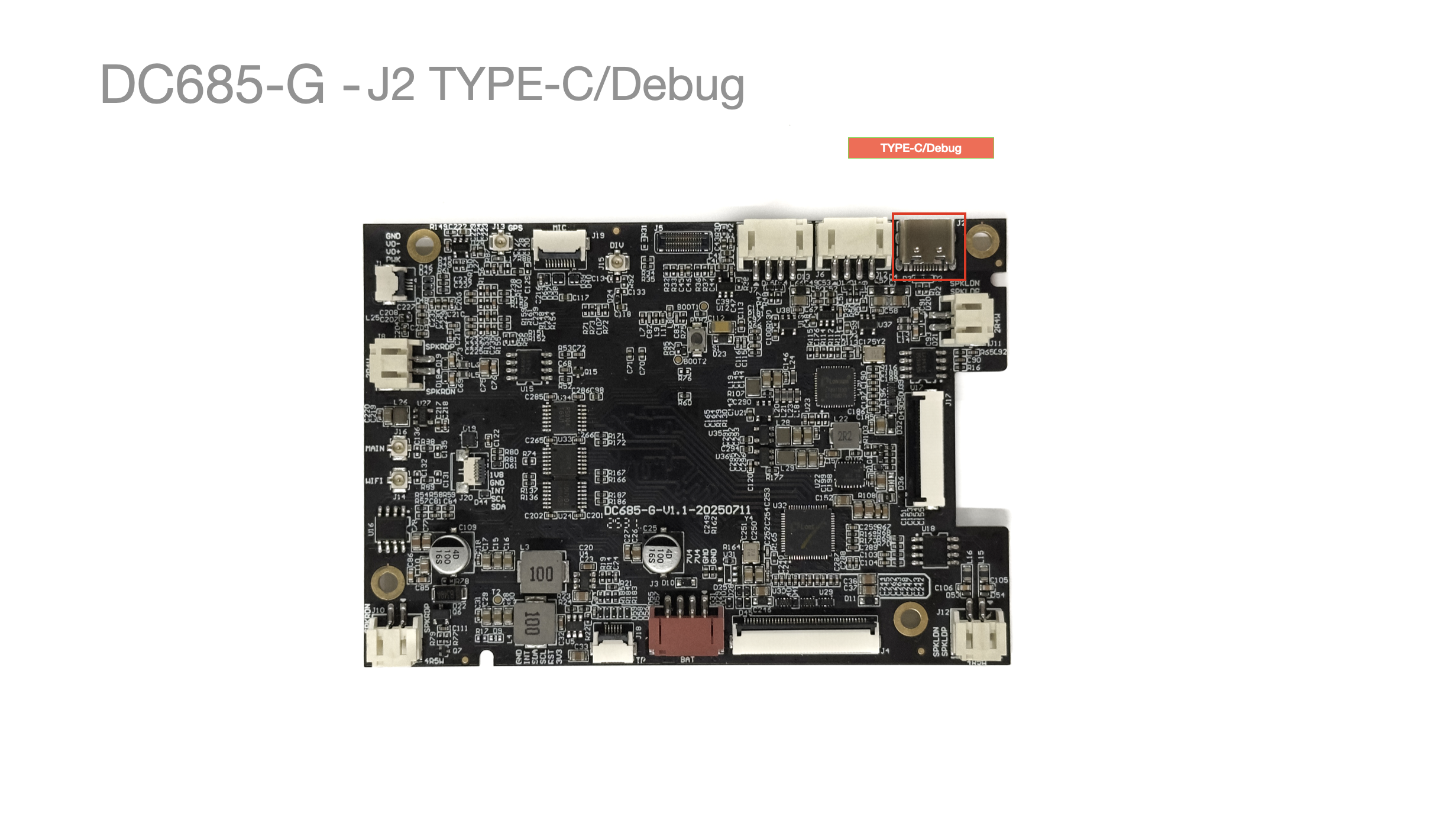
- Part model: MC-311D, used for flashing and debugging
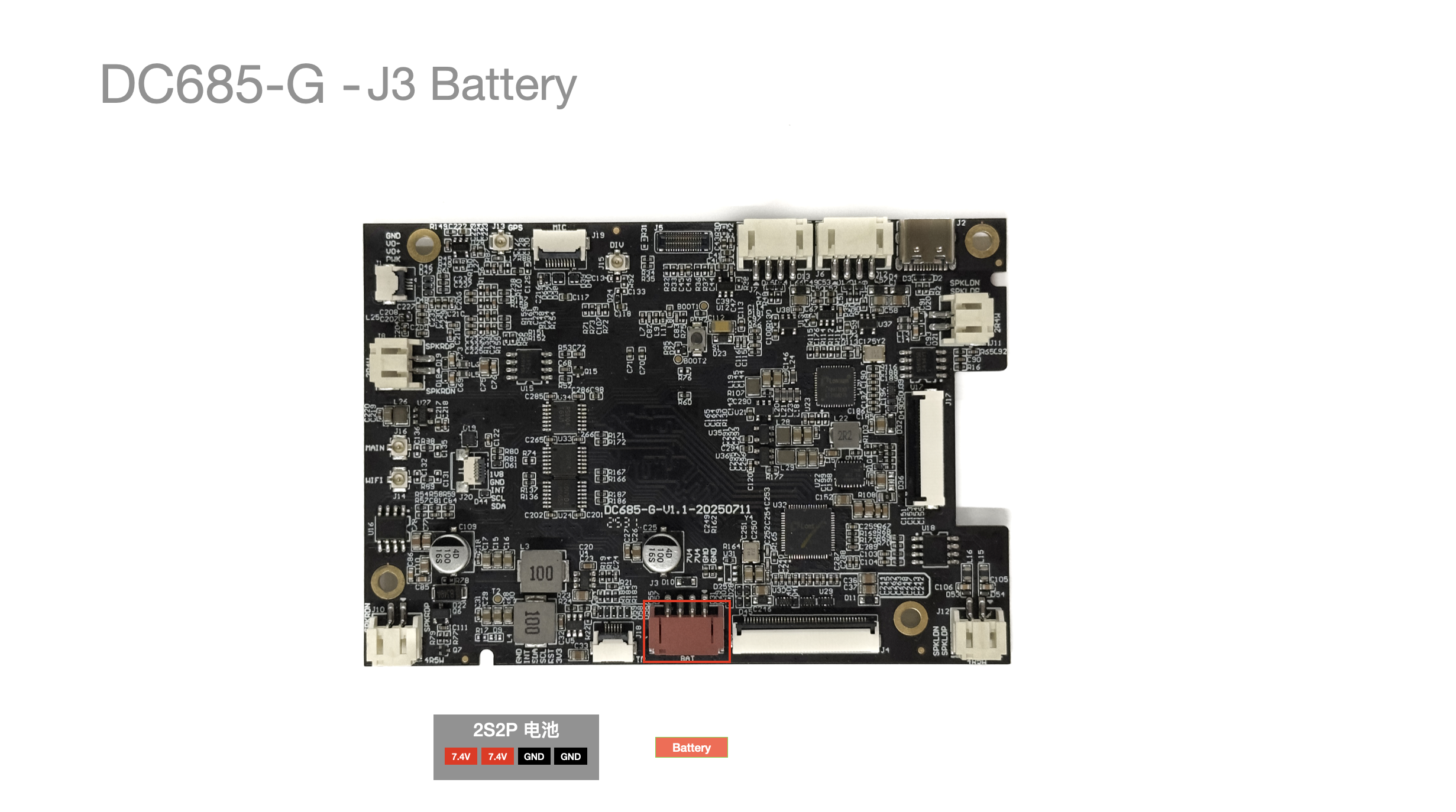
J3 BAT Battery
-
Part model: A2001WR-S-4, SMD 2.0mm socket, red, 4PIN, horizontal/gold-plated pins
-
Battery supports 5000mAh 0.2C discharge, 2S2P, maximum charging current 2A; two-series (two 4.2V batteries in series) polymer or lithium batteries
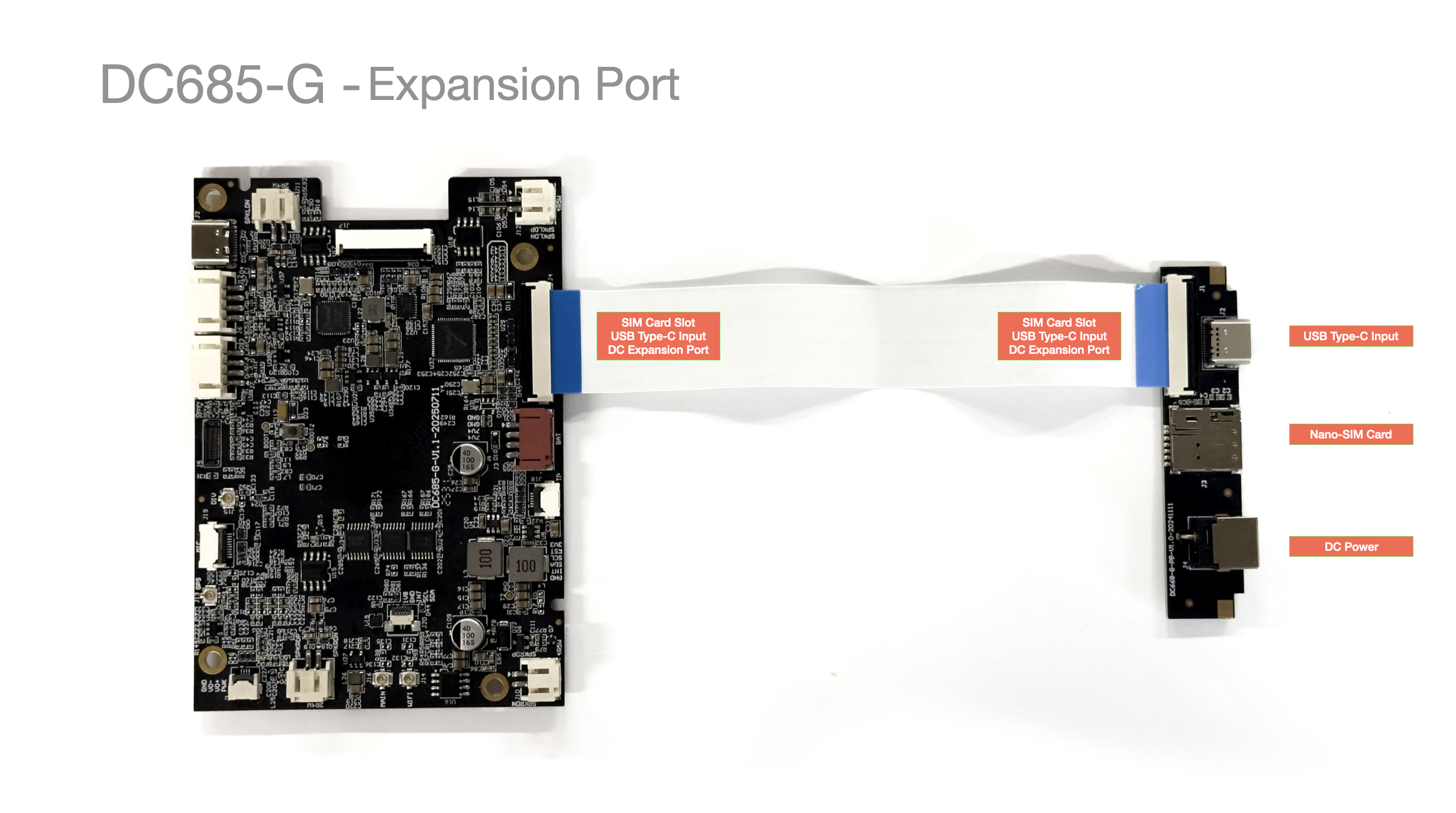
J4: SIM\Type-c IN\DC Expansion Interface
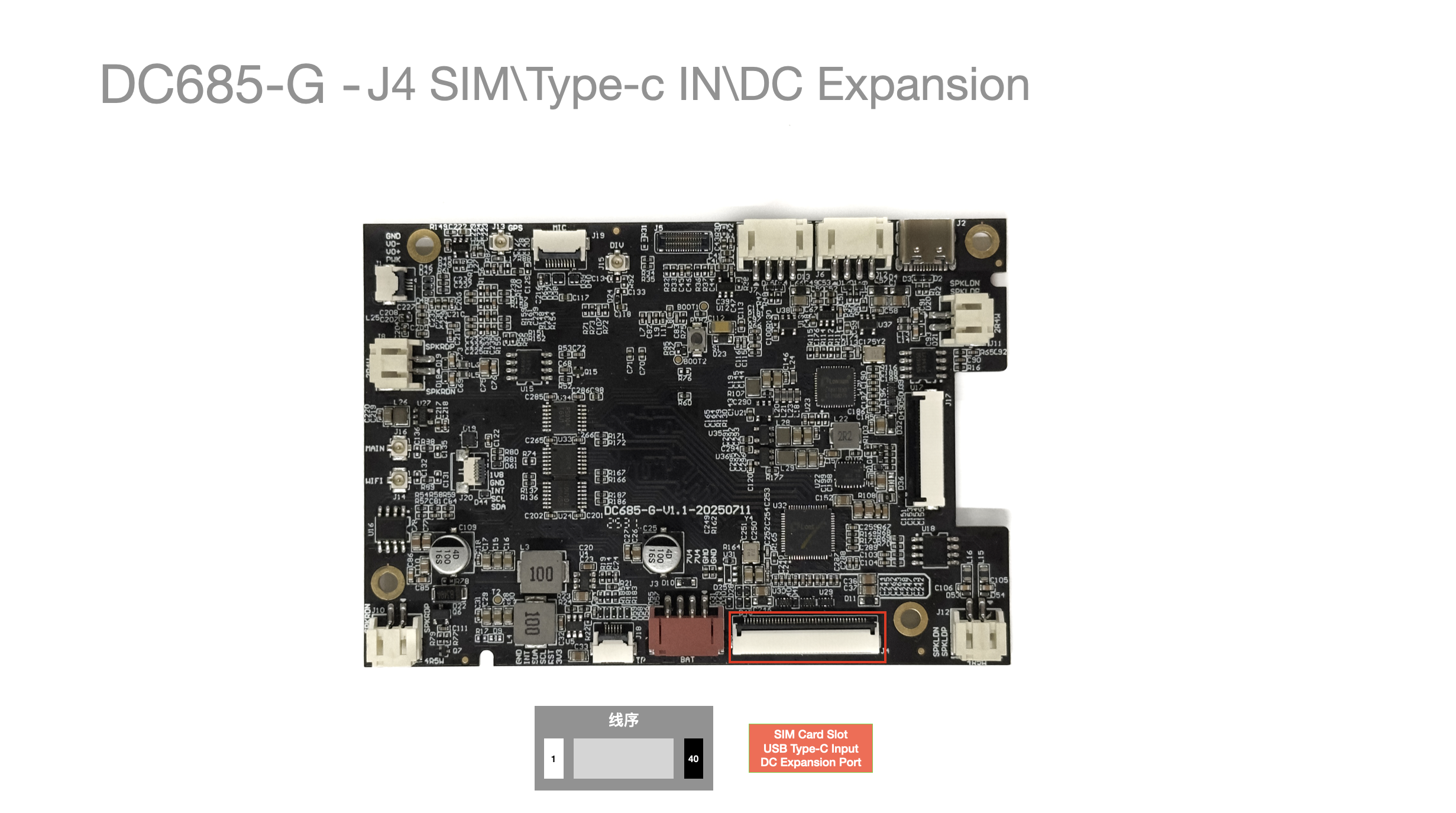
- Part model: FPC_OK-F505-40325W
| Pin No. | Pin Description | Remarks |
|---|---|---|
| 1 | SIM_DET_4G | SIM |
| 2 | SIM_VDD | SIM |
| 3 | SIM_RST_4G | SIM |
| 4 | SIM_DATA_4G | SIM |
| 5 | SIM_CLK_4G | SIM |
| 6 | GND | SIM |
| 7 | VBUS_DP | Type-c in |
| 8 | VBUS_DP | Type-c in |
| 9 | VBUS_DP | Type-c in |
| 10 | VBUS_DP | Type-c in |
| 11 | GND | Type-c in |
| 12 | DP_TX0_P | Type-c in |
| 13 | DP_TX0_N | Type-c in |
| 14 | GND | Type-c in |
| 15 | DP_RX0_P | Type-c in |
| 16 | DP_RX0_N | Type-c in |
| 17 | DP_CC1 | Type-c in |
| 18 | GND | Type-c in |
| 19 | DP_USB_P | Type-c in |
| 20 | DP_USB_N | Type-c in |
| 21 | GND | Type-c in |
| 22 | DP_AUX_P | Type-c in |
| 23 | DP_AUX_N | Type-c in |
| 24 | GND | Type-c in |
| 25 | DP_RX1_N | Type-c in |
| 26 | DP_RX1_P | Type-c in |
| 27 | GND | Type-c in |
| 28 | DP_CC2 | Type-c in |
| 29 | DP_TX1_N | Type-c in |
| 30 | DP_TX1_P | Type-c in |
| 31 | GND | DC |
| 32 | GND | DC |
| 33 | GND | DC |
| 34 | GND | DC |
| 35 | GND | DC |
| 36 | 12V | DC |
| 37 | 12V | DC |
| 38 | 12V | DC |
| 39 | 12V | DC |
| 40 | 12V | DC |
J5 MIPI
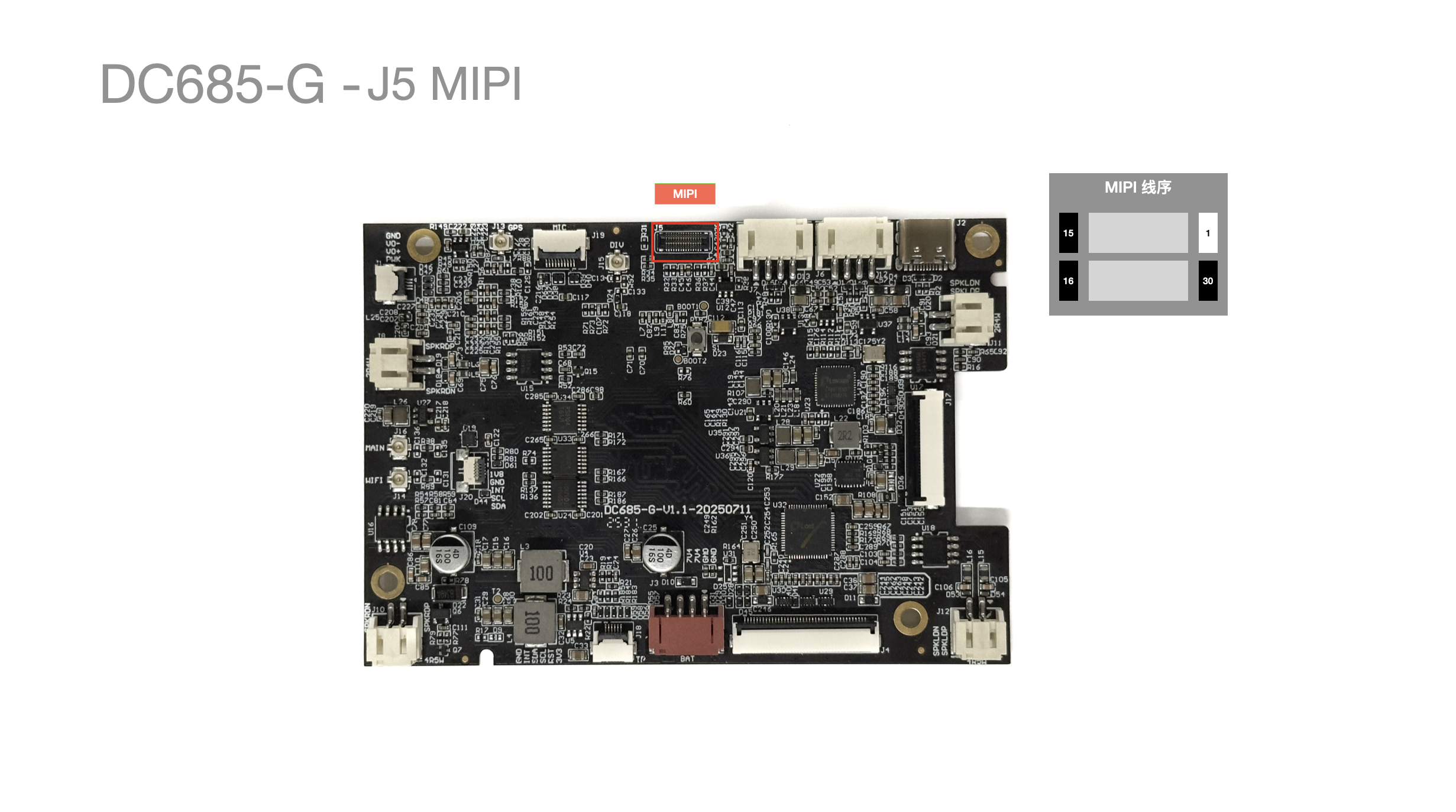
- Part model: YXT-BB10-30S-02
| Pin No. | Pin Description | Remarks |
|---|---|---|
| 1 | GND | |
| 2 | MCP | |
| 3 | MCN | |
| 4 | GND | |
| 5 | MDP2 | |
| 6 | MDN2 | |
| 7 | GND | |
| 8 | MDP0 | |
| 9 | MDN0 | |
| 10 | GND | |
| 11 | MDP3 | |
| 12 | MDN3 | |
| 13 | GND | |
| 14 | MDP1 | |
| 15 | MDN1 | |
| 16 | GND | |
| 17 | ID(DOVDD) | |
| 18 | GND | |
| 19 | PWDN | |
| 20 | NC(RESET) | |
| 21 | SDA | |
| 22 | SCL | |
| 23 | DVDD_1V2 | |
| 24 | GND | |
| 25 | MCLK | |
| 26 | GND | |
| 27 | DOVDD1V8 | |
| 28 | GND | |
| 29 | AVDD_2V95 | |
| 30 | AF_VDD_2V8 | |
| 31 | GND | |
| 32 | GND | |
| 33 | GND | |
| 34 | GND |
J6/J7 USB-A 2.0 Interfaces
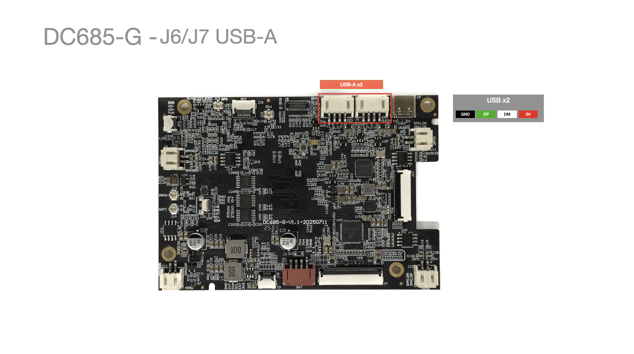
- Part model: A2001WR-S-4, SMD 2.0mm socket, off-white, 4PIN, horizontal/gold-plated pins
- USB2.0 high-speed (HS) interface.
J8/J10/J11/J12 Speaker (Power Amplifier)
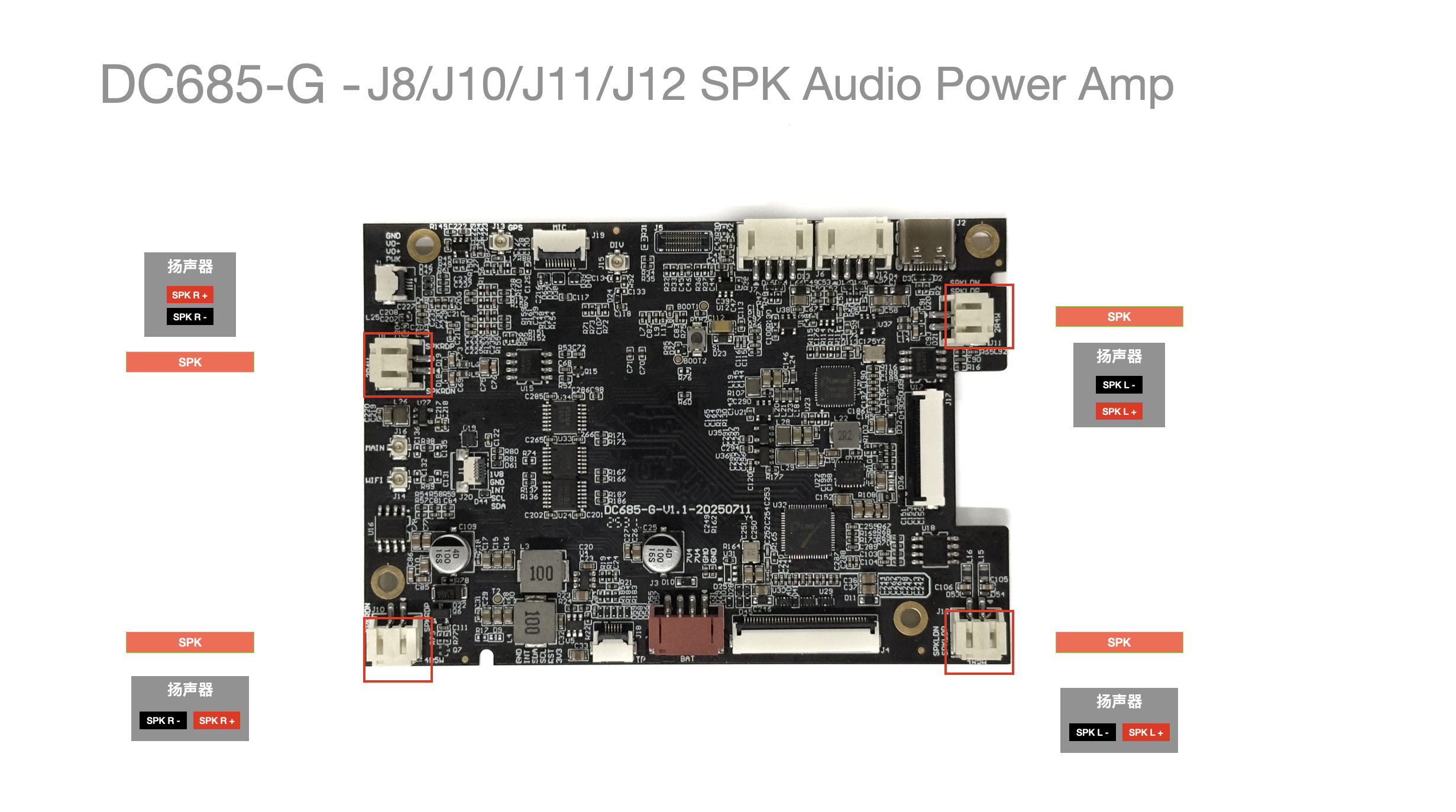
-
Part model: A2001WR-S-2, SMD 2.0mm socket, off-white, 2PIN, horizontal/gold-plated pins
-
4-channel power amplifier output
| Interface | Pin No. | Pin Description | Remarks |
|---|---|---|---|
| J8 | 1 | R- | Connect to a 2R/4W speaker |
| J8 | 2 | R+ | Connect to a 2R/4W speaker |
| J10 | 1 | R+ | Connect to a 4R/5W speaker |
| J10 | 2 | R- | Connect to a 4R/5W speaker |
| J11 | 1 | L- | Connect to a 2R/4W speaker |
| J11 | 2 | L+ | Connect to a 2R/4W speaker |
| J12 | 1 | L+ | Connect to a 4R/5W speaker |
| J12 | 2 | L- | Connect to a 4R/5W speaker |
J13/J14/J15/J16 Antenna Interfaces
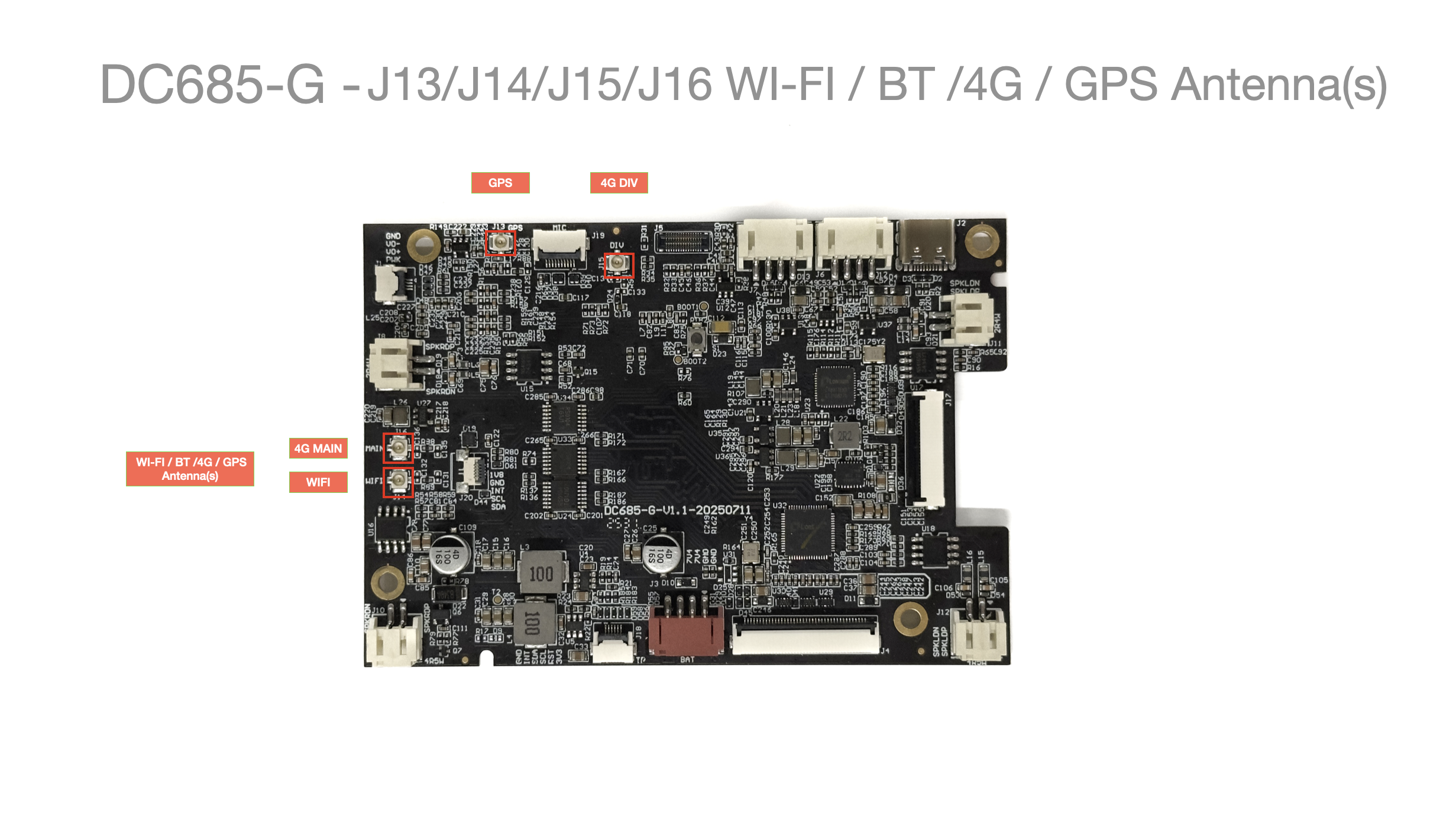
- Part model: UFL-R-SMT-1, 1st generation SMD RF connector
| Interface | Antenna Type | Remarks |
|---|---|---|
| J13 | GPS antenna | |
| J14 | WIFI antenna | |
| J15 | 4G main antenna | |
| J16 | 4G auxiliary antenna |
J17 eDP Interface
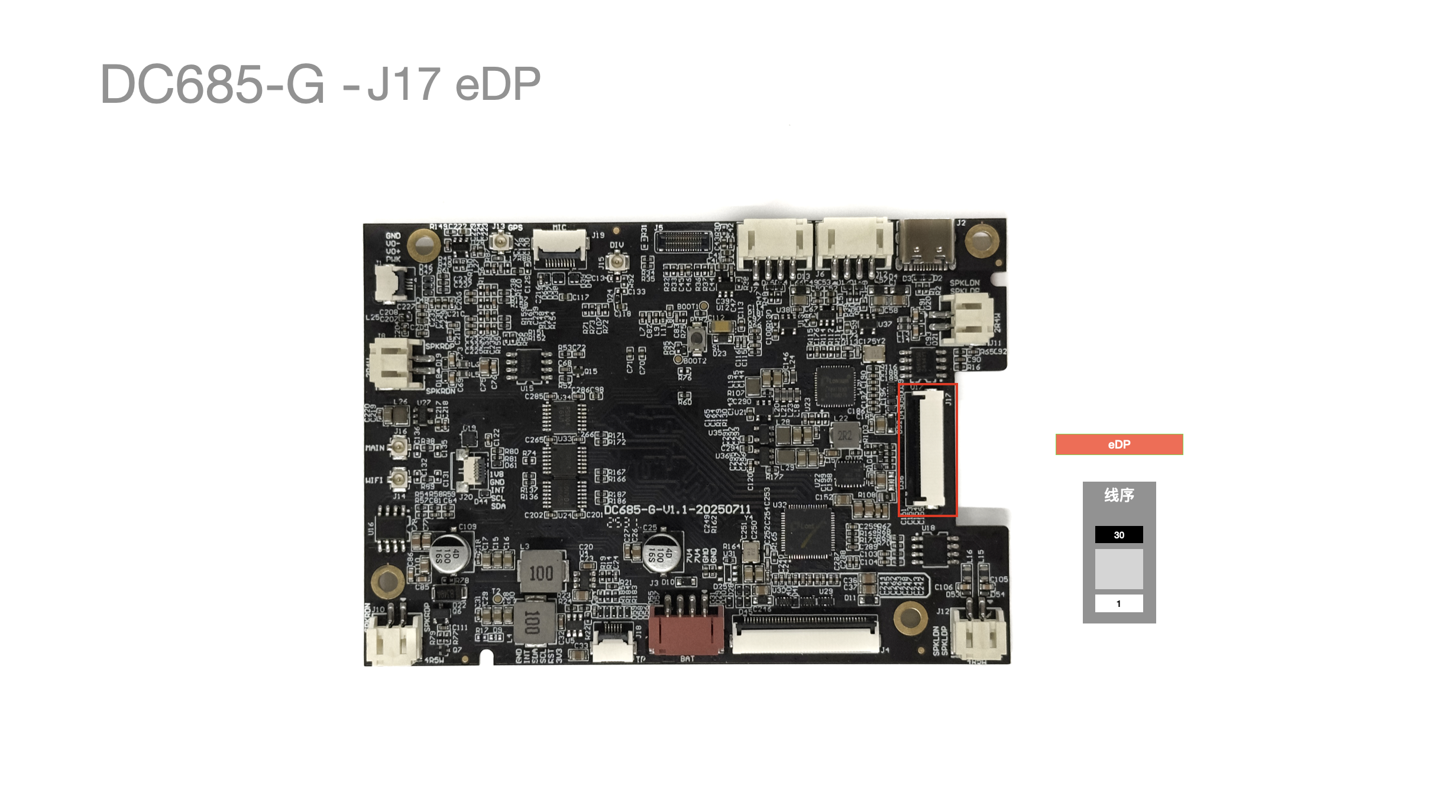
- Part model: FPC_OK-F505-30325W
- Supports up to 2560*1200@60FPS
J18 I2C Touch Interface
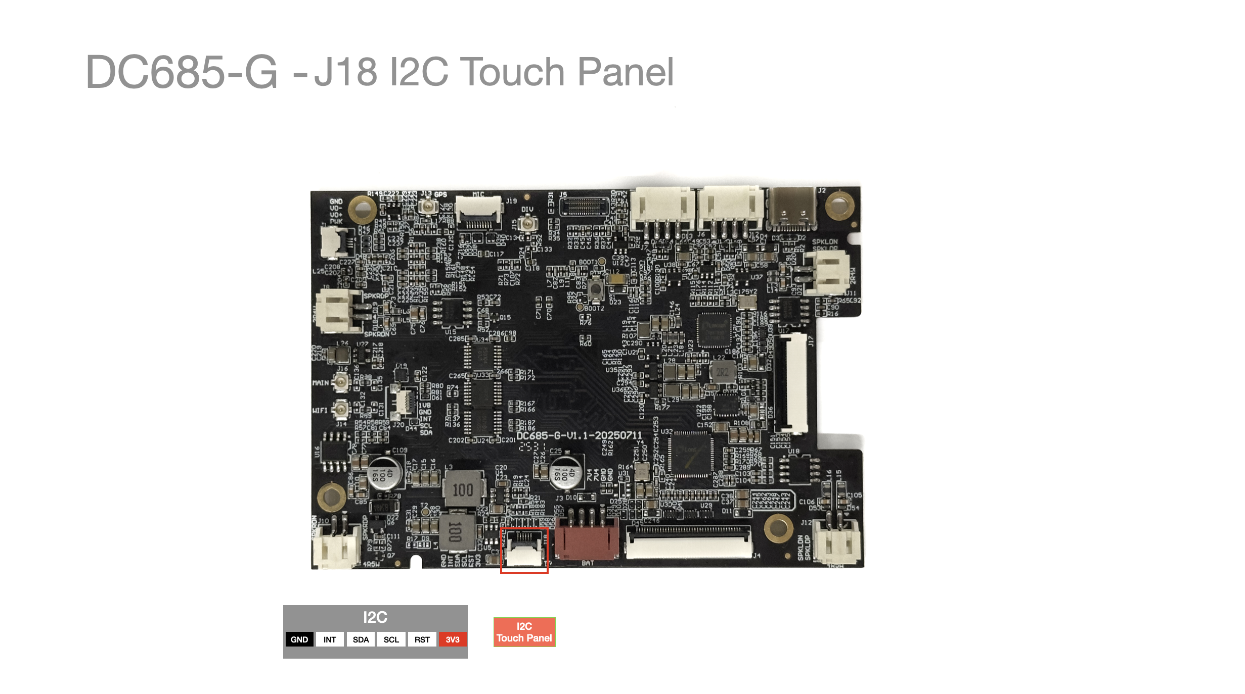
| Pin No. | Pin Description | Remarks |
|---|---|---|
| 1 | GND | |
| 2 | TP1_INT1 | |
| 3 | TP1_SDA | |
| 4 | TP1_SCL | |
| 5 | TP1_RST | |
| 6 | 3V3 |
J19 MIC
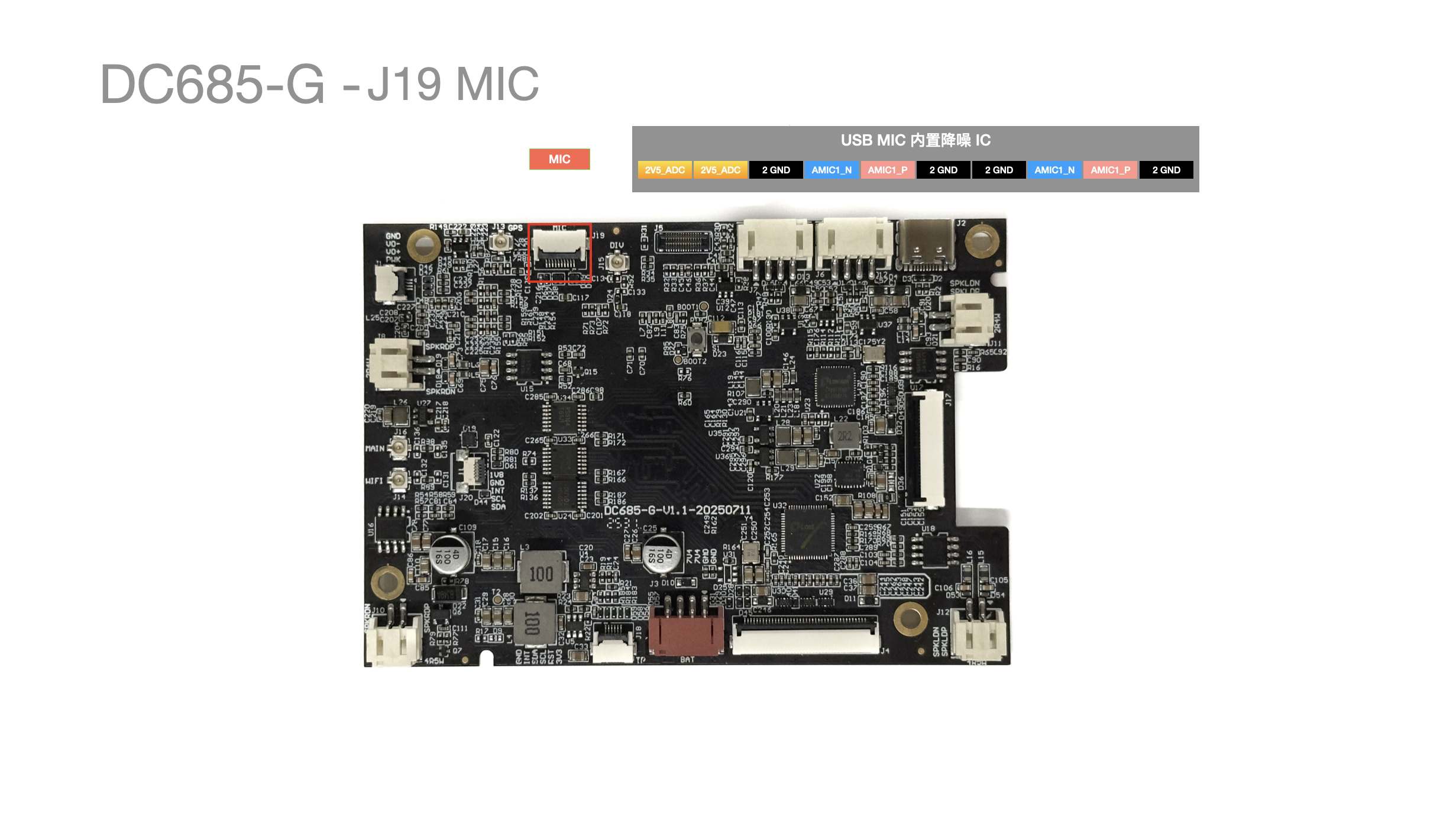
- Part model: AFC24-S10FIA-HF
| Pin No. | Pin Description | Remarks |
|---|---|---|
| 1 | GND | USB MIC, built-in noise reduction IC |
| 2 | AMIC1_P | USB MIC, built-in noise reduction IC |
| 3 | AMIC1_N | USB MIC, built-in noise reduction IC |
| 4 | GND | USB MIC, built-in noise reduction IC |
| 5 | GND | USB MIC, built-in noise reduction IC |
| 6 | AMIC0_P | USB MIC, built-in noise reduction IC |
| 7 | AMIC0_N | USB MIC, built-in noise reduction IC |
| 8 | GND | USB MIC, built-in noise reduction IC |
| 9 | 2V5_ADC | USB MIC, built-in noise reduction IC |
| 10 | 2V5_ADC | USB MIC, built-in noise reduction IC |
J20 I2C Interface
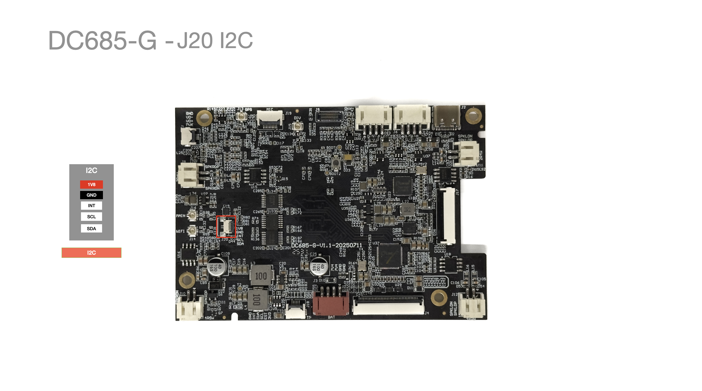
- For an external gyroscope
| Pin No. | Pin Description | Remarks |
|---|---|---|
| 1 | 1V8 | |
| 2 | GND | |
| 3 | INT | |
| 4 | SCL | |
| 5 | SDA |
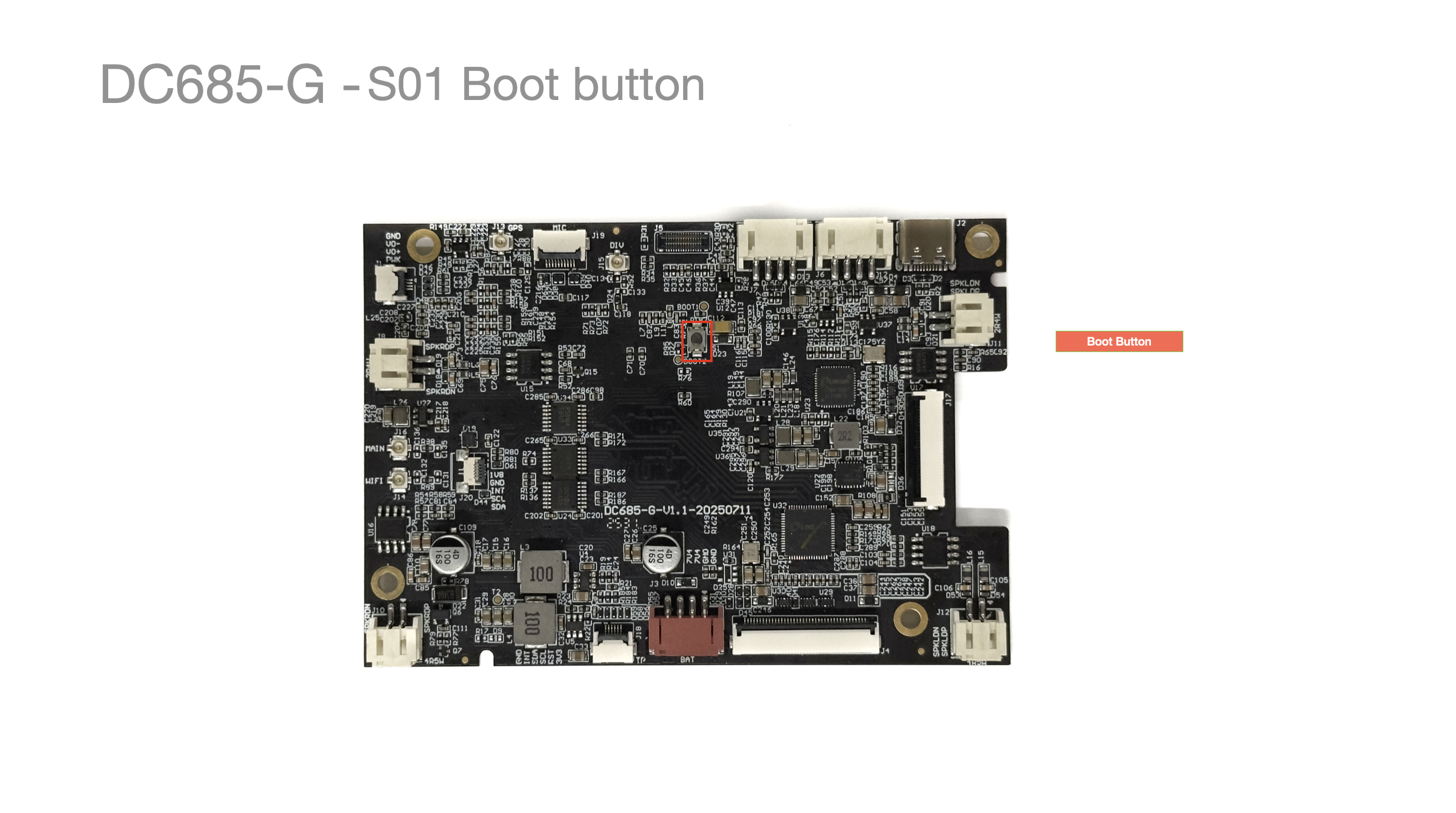
S1 Boot Button
-
Used to enter flashing mode.
-
Usage: press and hold this button before powering on, then release after powering on to enter flashing mode.
Debug Interface
Soldering to the test points is required
Schematic
Expansion Interfaces
Expansion Interface Preview
The expansion boards all use standard interfaces and are not described separately