Interface Definition

The DC690H provides a rich set of interfaces, as shown in the following diagram:
Overall Interface Definition
Overall Device Interfaces
J1 Power Supply
Connection Method
Interface Pin Definition
| J1 Pin No. | Pin Description | Wire Color (Reference) | Remarks |
|---|---|---|---|
| 1 | 24V | Red | Operating voltage 12-24V |
| 2 | 24V | Red | Operating voltage 12-24V |
| 3 | GND | Black | Ground |
| 4 | GND | Black | Ground |
Connect to 12-24V Power Supply
- Supports
DC 12-24V 4PINpower connector
J2/J41 DC 5525 connector optional:
Not installed by default
Measured Power Consumption
-
Test Method:
- Flash the default
Androidfirmware - Power on normally, unlock the screen and perform no other operations
- Measure only the mainboard power supply, backlight not connected.
- Flash the default
| State | Voltage | Current | Power | Remarks |
|---|---|---|---|---|
| Normal boot, no screen connected | 12.4V | 0.1A | Standby 1.8-2.5W | Measurement accuracy 0.1 |
J3 RTC Battery
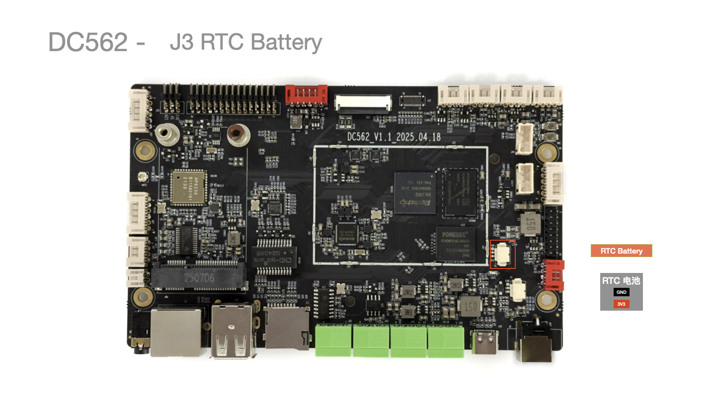
| Pin No. | Pin Description | Wire Color (Reference) |
|---|---|---|
| 1 | GND | Black |
| 2 | 3V3 | Red |
J4 SYS FAN (Cooling Fan)
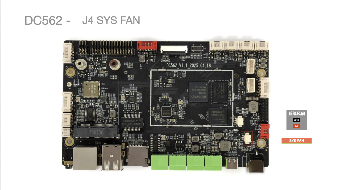
| Pin No. | Pin Description | Wire Color (Reference) |
|---|---|---|
| 1 | GND | Black |
| 2 | 5V | Red |
J5 Ethernet Interface
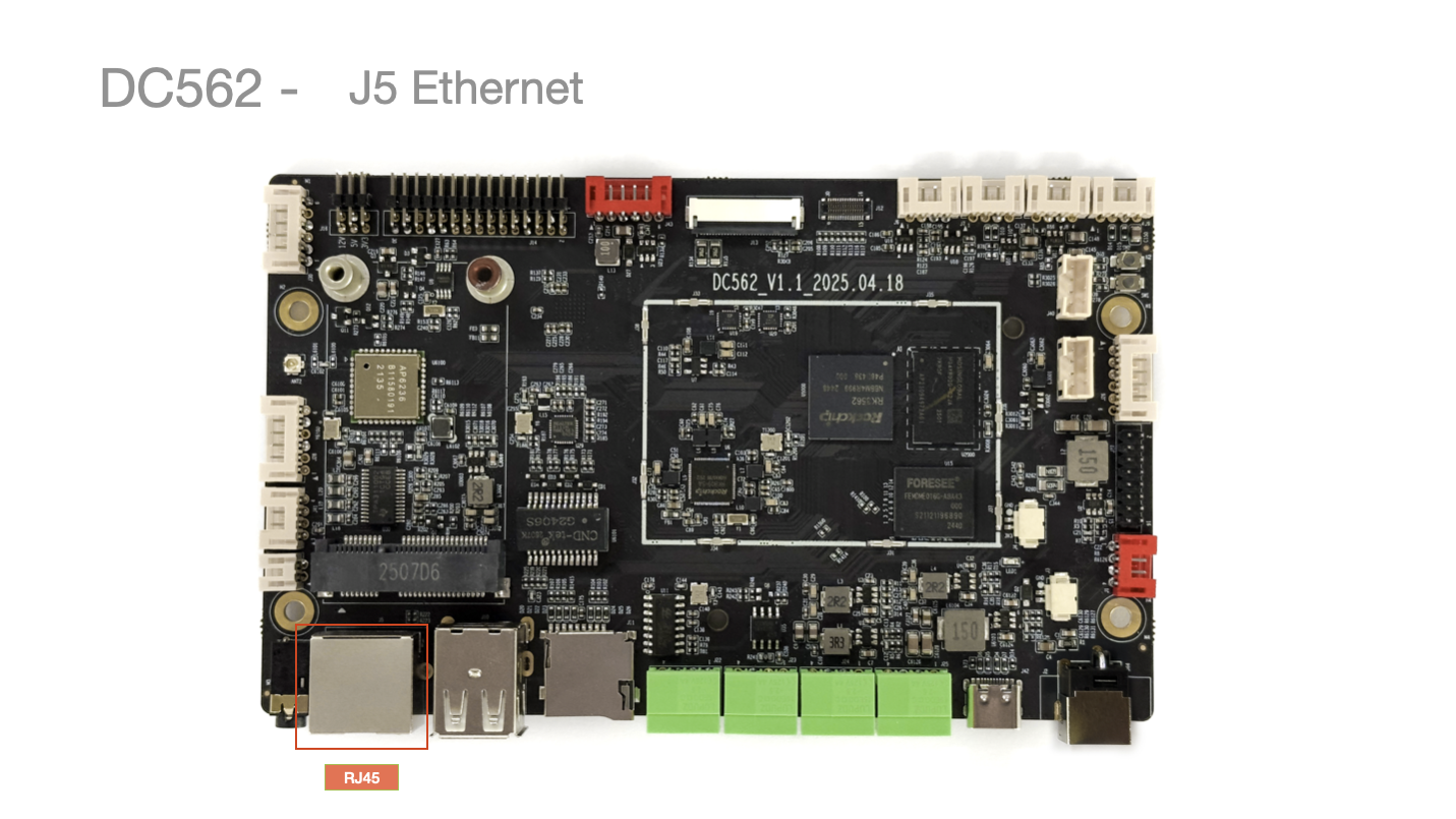
- Auto-negotiating Gigabit Ethernet, supports 10/100/1000Mbps auto-negotiation
J6/J7/J8/J9 USB 4-PIN Interface
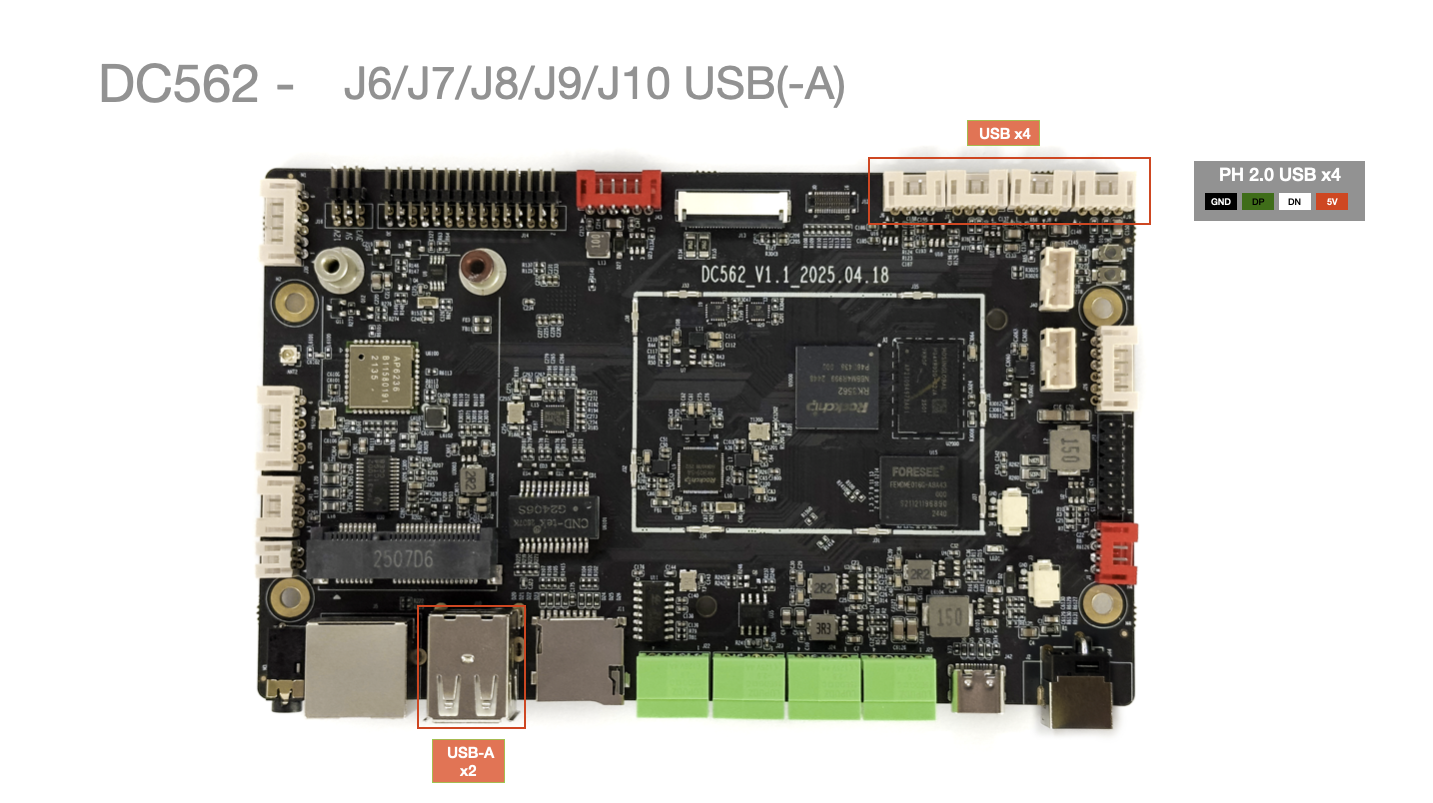
| Pin No. | Pin Description | Wire Color (Reference) | Remarks |
|---|---|---|---|
| 1 | GND | Black | Ground |
| 2 | DP | Green | Data Positive |
| 3 | DM | White | Data Negative |
| 4 | 5V | Red | 5V Power |
- Supports 4 USB PH2.0 ports
J10 USB-A 3.0 Interface
- Supports 2 standard USB-A 2.0 interfaces
J11 TF-Card Interface
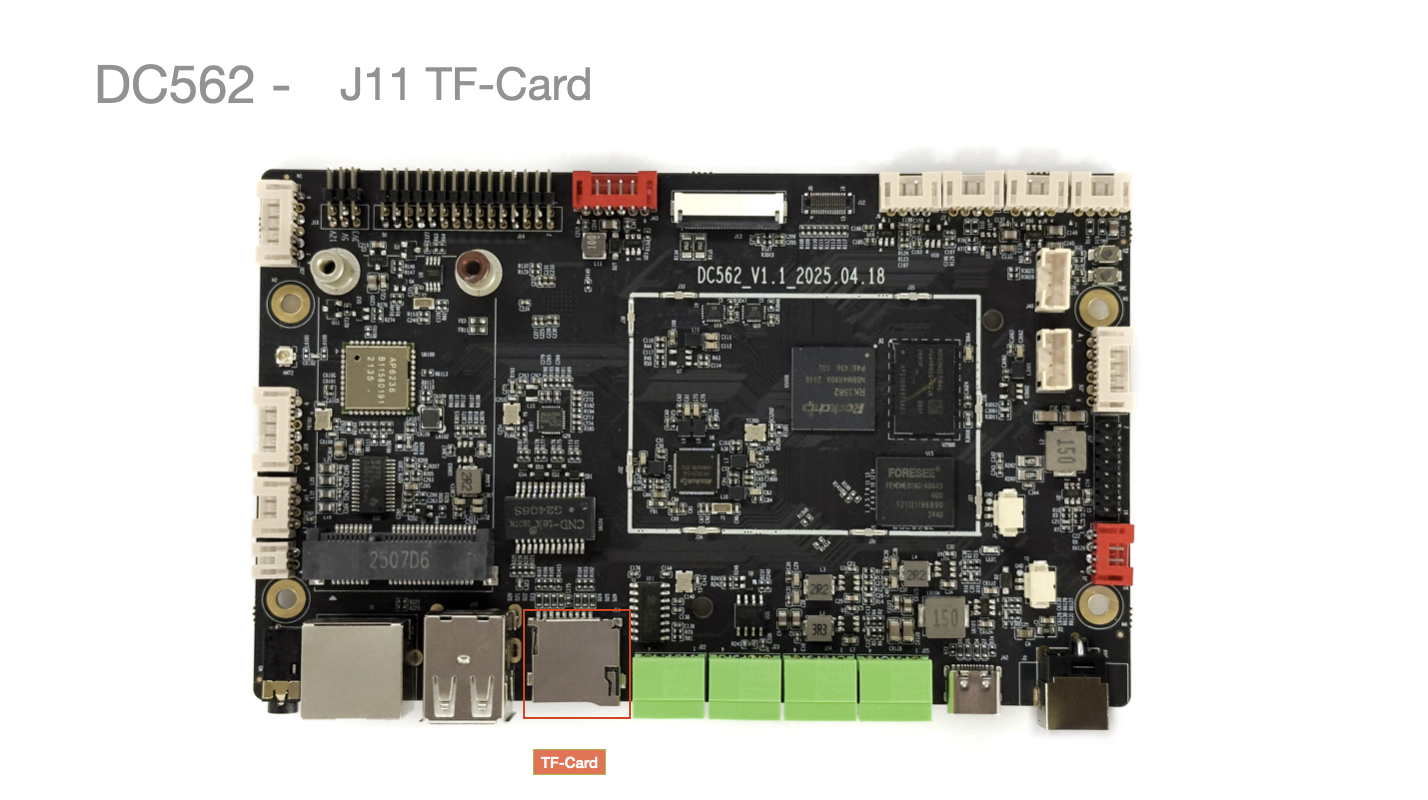
Maximum tested capacity: 256G, theoretically supports 512G
J12 MIPI Camera Interface
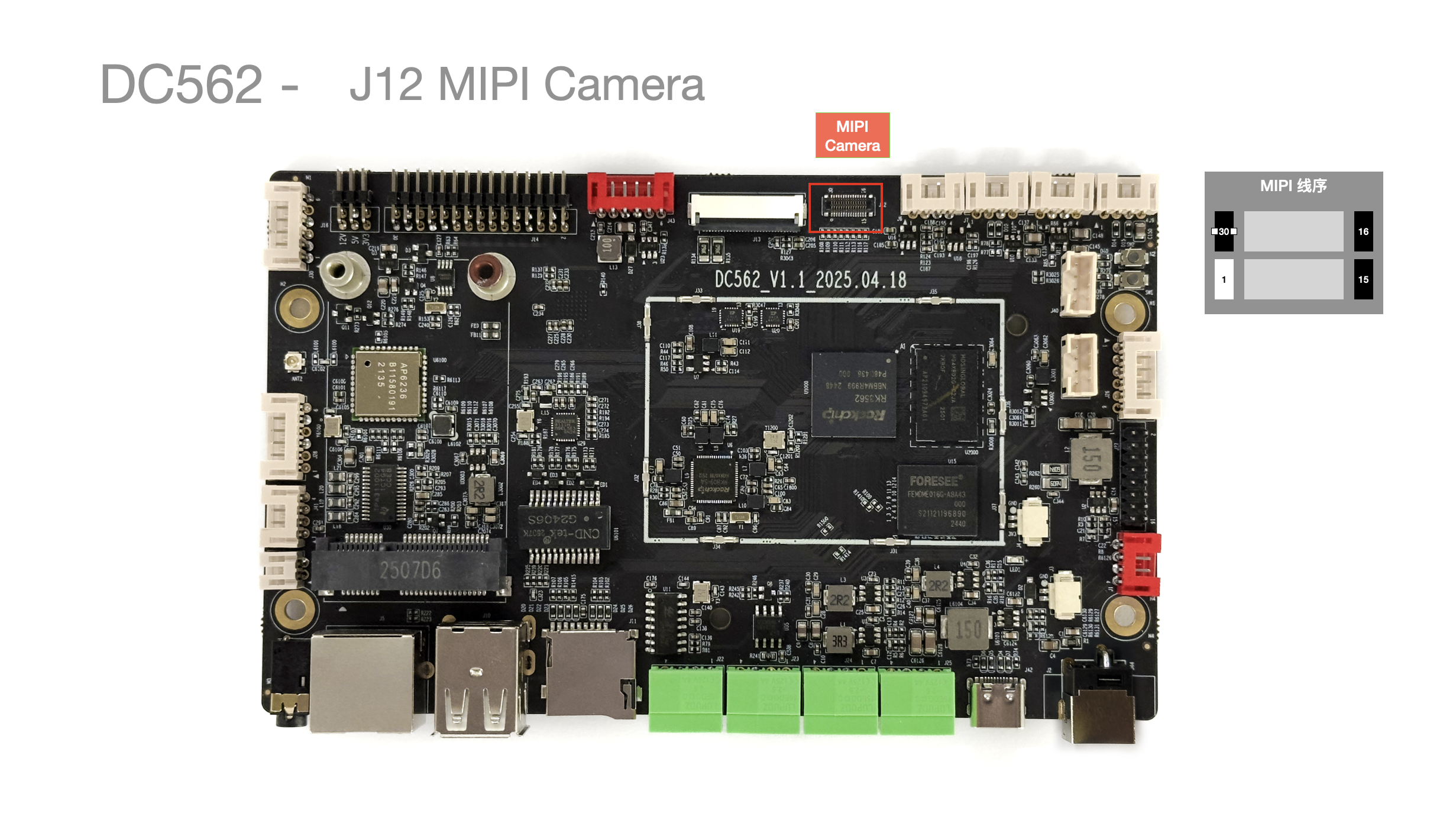
- Connector Model: YXT-BB10-30S-02
J13 MIPI DSI Display Interface
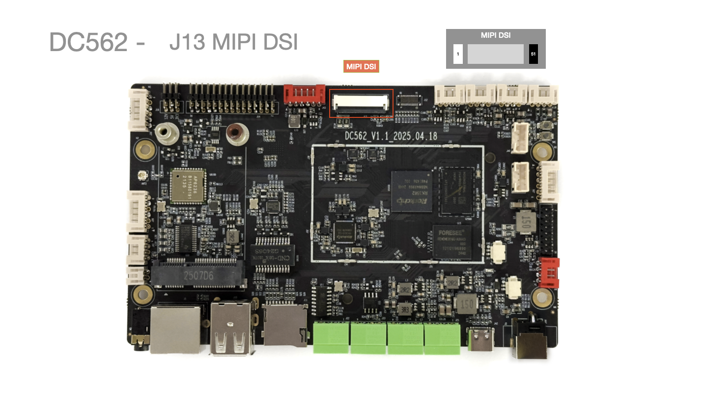
- Connector Model: con30
J14 Dual-Channel LVDS Interface
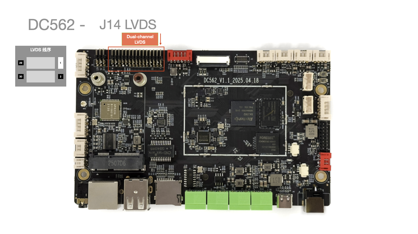
- LCM Interface: Dual Port LVDS interface, maximum resolution (1920*1080@60fps)
J16 LVDS Power Selection
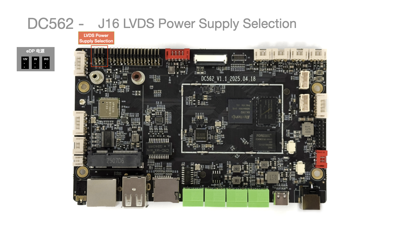
- Pay attention to the
output voltage to avoiddamaging the screen
J19 3.5mm Headphone Jack
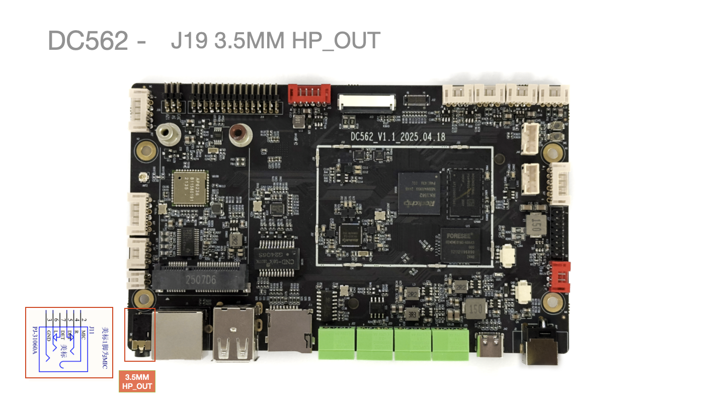
3.5mm Interface: US Standard (CTIA)
J21 SIM Card Slot
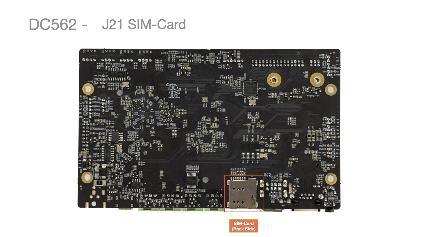
Supports standard SIM card
J22/J23 RS-232 Interface
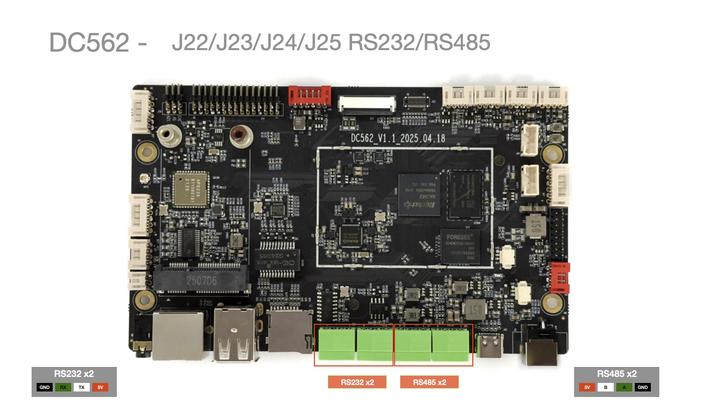
| Pin No. | Pin Description | Remarks |
|---|---|---|
| 1 | GND | UART 4/7 |
| 2 | RX | UART 4/7 (Receive) |
| 3 | TX | UART 4/7 (Transmit) |
| 4 | 5V | UART 4/7 |
J24/J25 RS-485 Interface
| Pin No. | Pin Description | Remarks |
|---|---|---|
| 1 | 5V | UART 8/6 |
| 2 | B | UART 8/6 (Data Line B/-) |
| 3 | A | UART 8/6 (Data Line A/+) |
| 4 | GND | UART 8/6 |
J26 SPI Interface
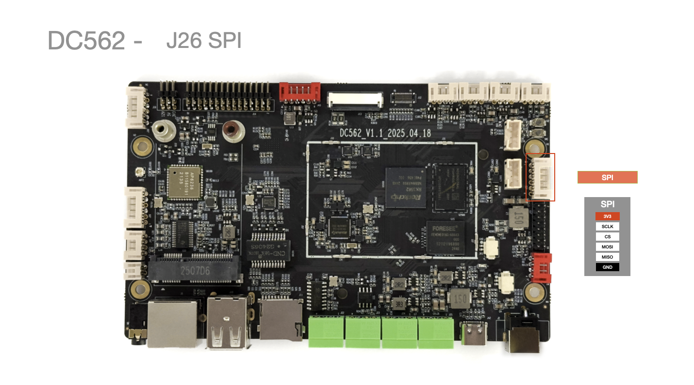
| Pin No. | Pin Description | Remarks |
|---|---|---|
| 1 | 3V3 | SPI1 (Power) |
| 2 | SPI_CLK | SPI1 (Clock) |
| 3 | CS | SPI1 (Chip Select) |
| 4 | MOSI | SPI1 (Master Out Slave In) |
| 5 | MISO | SPI1 (Master In Slave Out) |
| 6 | GND | SPI1 (Ground) |
J27 DI x4 / DO x4 / CAN / 12V Interface
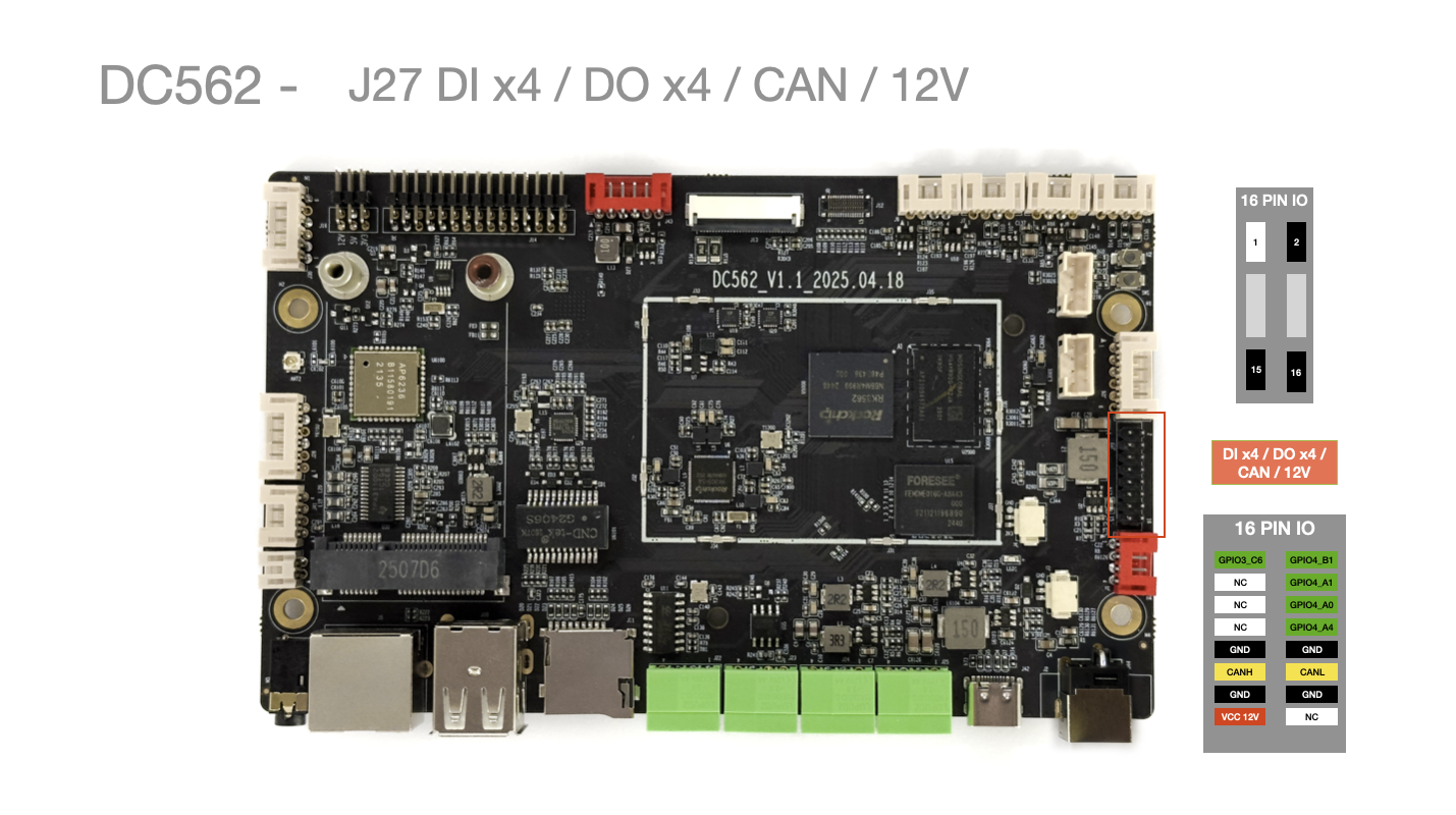
| Pin No. | Pin Description | Remarks |
|---|---|---|
| 1 | GPIO3_C6 | Digital Input/Output |
| 2 | GPIO4_B1 | Digital Input/Output |
| 3 | NC | Not Connected |
| 4 | GPIO4_A1 | Digital Input/Output |
| 5 | NC | Not Connected |
| 6 | GPIO4_A0 | Digital Input/Output |
| 7 | NC | Not Connected |
| 8 | GPIO_A4 | Digital Input/Output |
| 9 | GND | Ground |
| 10 | GND | Ground |
| 11 | CANH | CAN Bus High Line |
| 12 | CANL | CAN Bus Low Line |
| 13 | GND | Ground |
| 14 | GND | Ground |
| 15 | 12V Power Output | |
| 16 | NC | Not Connected |
J28 I2C Interface
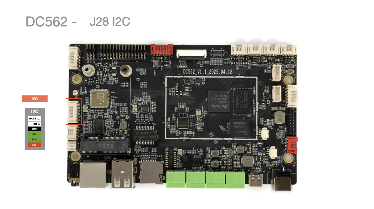
| Pin No. | Pin Description | Remarks |
|---|---|---|
| 1 | 3V3 | I2C2 (Power) |
| 2 | SDA | I2C2 (Data Line) |
| 3 | SCL | I2C2 (Clock Line) |
| 4 | GND | I2C2 (Ground) |
| 5 | NC | Not Connected |
| 6 | GPIO4_A0 | General Purpose Input/Output |
J30 Panel Button Interface
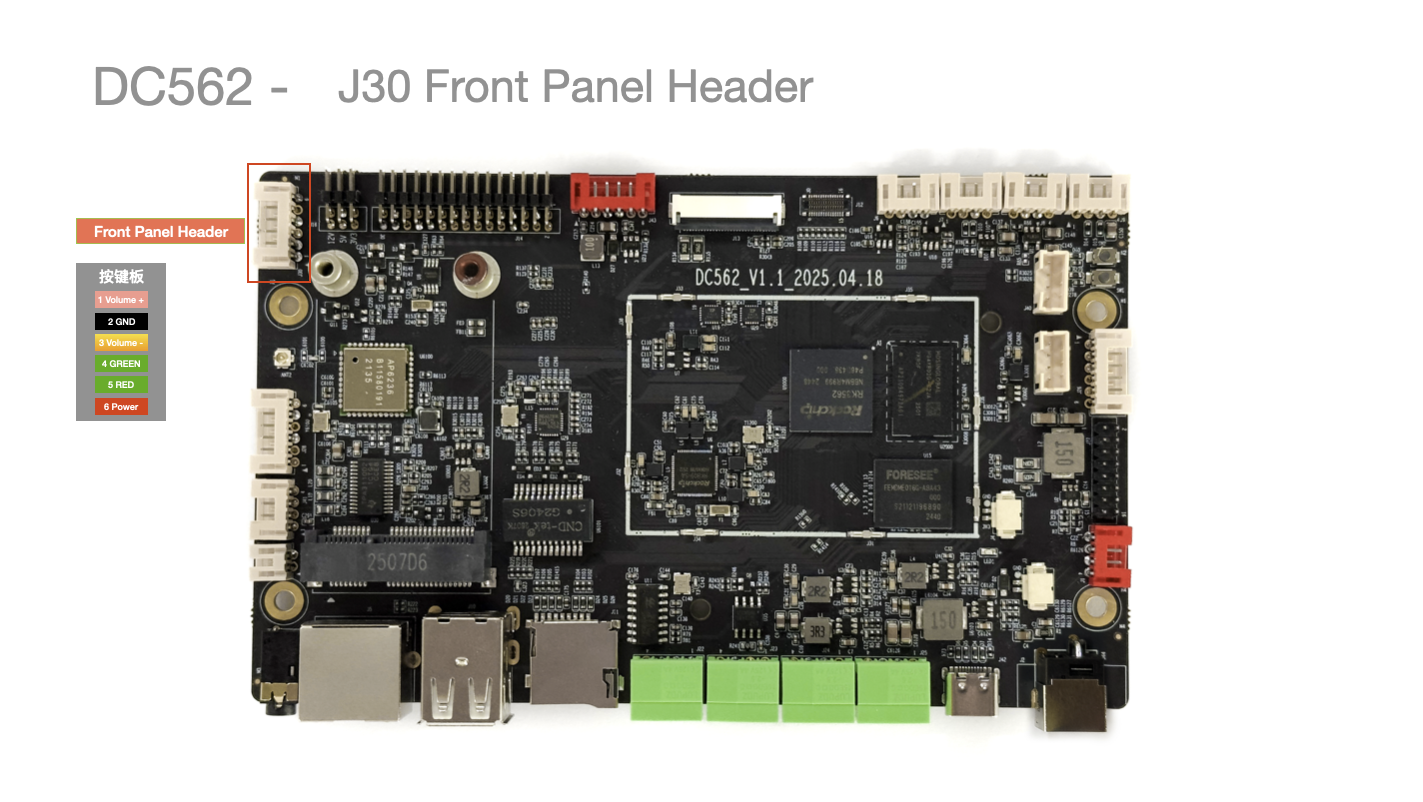
| Pin No. | Pin Description | Wire Color (Reference) | Remarks |
|---|---|---|---|
| 1 | Power | None | Short to Pin 5 GND for Power Button |
| 2 | LED_R | None | Connect to Pin 5 GND for Red LED control |
| 3 | LED_G | None | Connect to Pin 5 GND for Green LED control |
| 4 | Volume - | None | Short to Pin 5 GND for Volume Down |
| 5 | GND | Black | Ground |
| 6 | Volume + | None | Short to Pin 5 GND for Volume Up |
J39/J40 Debug Interface
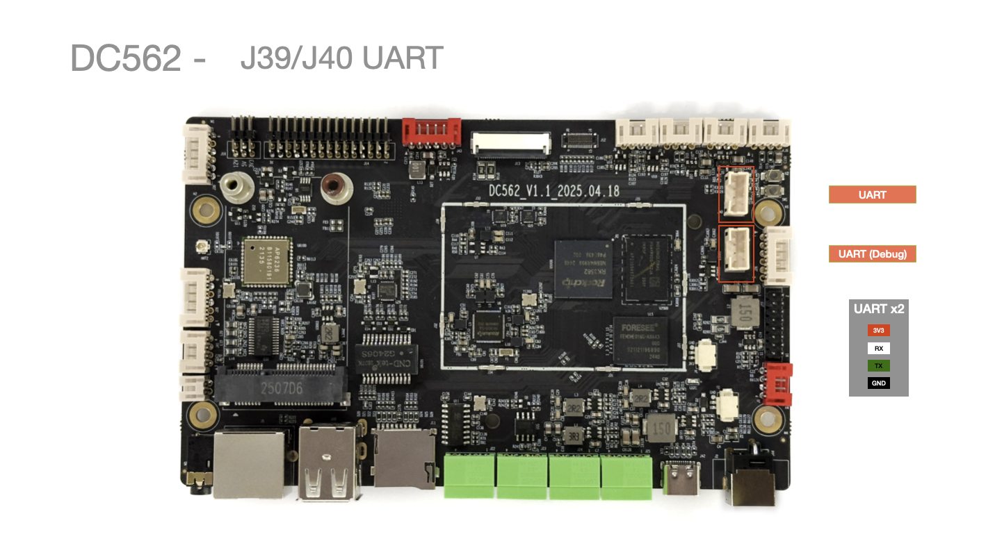
| J39 Pin No. | Pin Description | Wire Color (Reference) | Remarks |
|---|---|---|---|
| 1 | 3V3 | Red | Debug Power |
| 2 | UART0_RX | Green | Debug Receive |
| 3 | UART0_TX | Green | Debug Transmit |
| 4 | GND | Black | Debug Ground |
| J40 Pin No. | Pin Description | Wire Color (Reference) | Remarks |
|---|---|---|---|
| 1 | 3V3 | Red | UART9 Power |
| 2 | UART9_RX | Green | UART9 Receive |
| 3 | UART9_TX | Green | UART9 Transmit |
| 4 | GND | Black | UART9 Ground |
J42 TYPE-C Debug Interface
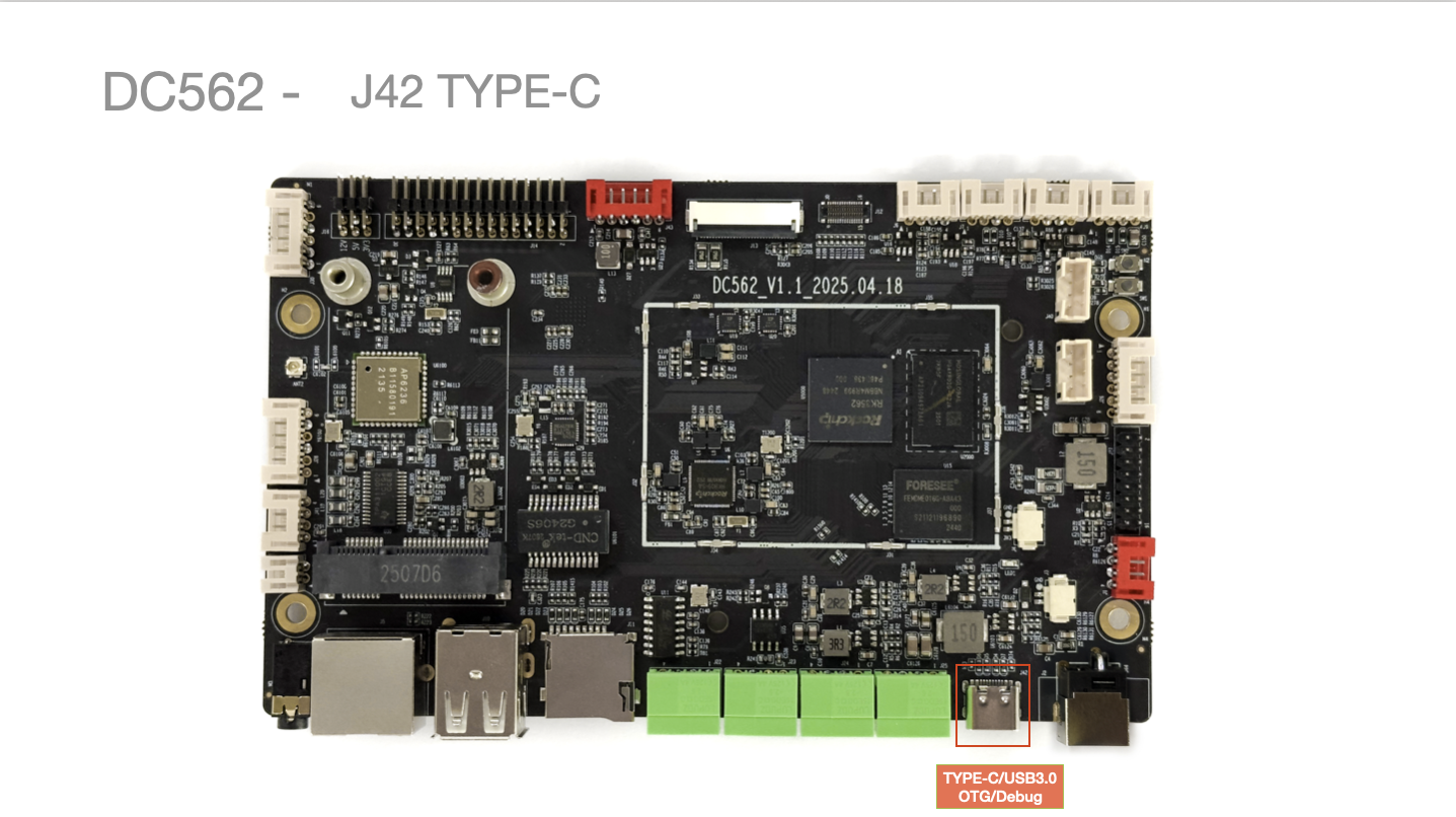
- TYPE-C Interface: Provides USB3.0 OTG function.
MIC1 2-Pin Microphone Interface
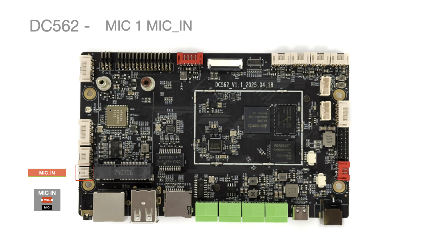
| Pin No. | Pin Description | Wire Color (Reference) |
|---|---|---|
| 1 | MIC- | Black (Microphone Negative) |
| 2 | MIC+ | Red (Microphone Positive) |
SW01 / SW02 Update Key / Recovery Key
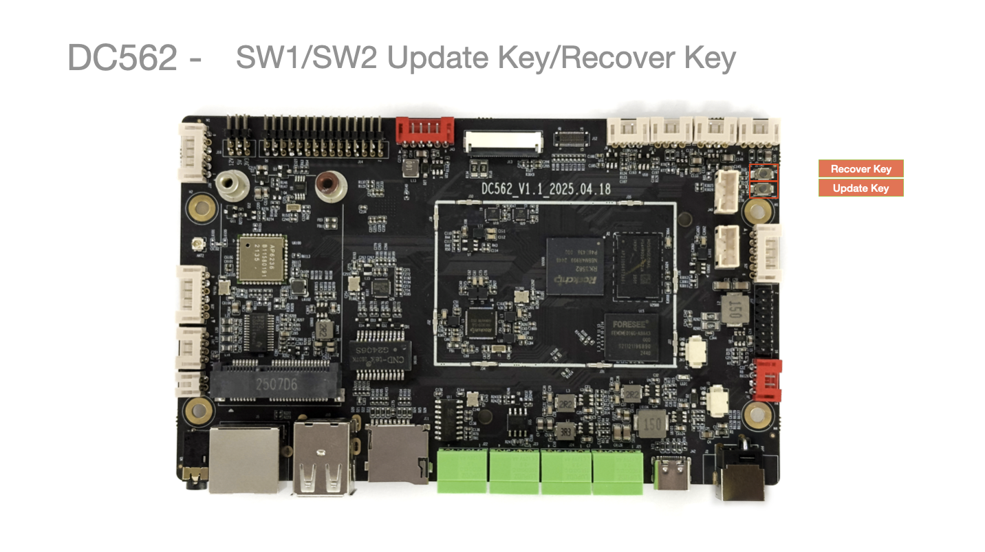
- Recovery Key: Press and hold during power-on to enter loader flashing mode.
- Update Key: Press and hold during power-on to enter maskrom flashing mode.