Interface Definitions

The IM2290 provides a rich set of interfaces, as shown in the following diagram:
/im2290/IM2290 /im2290/IM2290
Overall Interface Diagram
Overall Device Interfaces
J1/J2 Power Supply
Connection Method
Pin Definitions
| Pin No. | Pin Description | Wire Color (Reference) | Notes |
|---|---|---|---|
| 1 | GND | Black | Ground |
| 2 | GND | Black | Ground |
| 3 | 12V | Red | Operating Voltage 12V |
| 4 | 12V | Red | Operating Voltage 12V |
Connect to a 12V Power Supply
- Supports
DC 12V 4PINpower connector
Measured Power Consumption
-
Test Method:
- Flash the default
Androidfirmware. - Power on normally, unlock the screen, and perform no other operations.
- Measure only the motherboard power; the backlight is not connected.
- Flash the default
| State | Voltage | Current | Power | Notes |
|---|---|---|---|---|
| Normal boot, no screen connected | 12.4V | 0.1A | Standby 1.68-2.2W | Measurement accuracy 0.1 |
J3/J4/J19 UART/Debug Ports
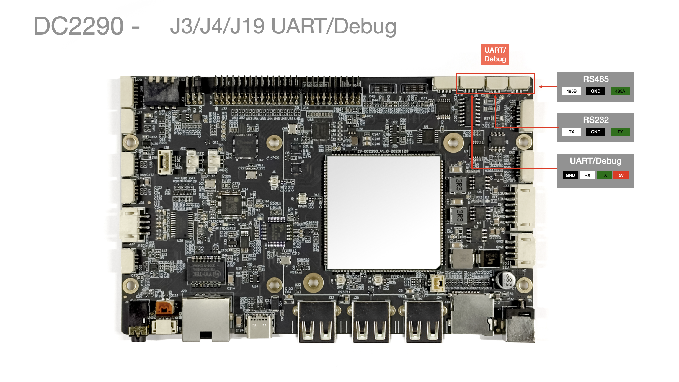
| Pin No. | Pin Description | Notes |
|---|---|---|
| J3 1 | RS232_TX | |
| J3 2 | GND | Ground |
| J3 3 | RS232_RX | |
| J4 1 | RS485_B | |
| J4 2 | GND | Ground |
| J4 3 | RS485_A | |
| J19 1 | GND | Ground |
| J19 2 | DBG_RXD | |
| J19 3 | DBG_TXD | |
| J19 4 | 5V |
J5 I2C Port
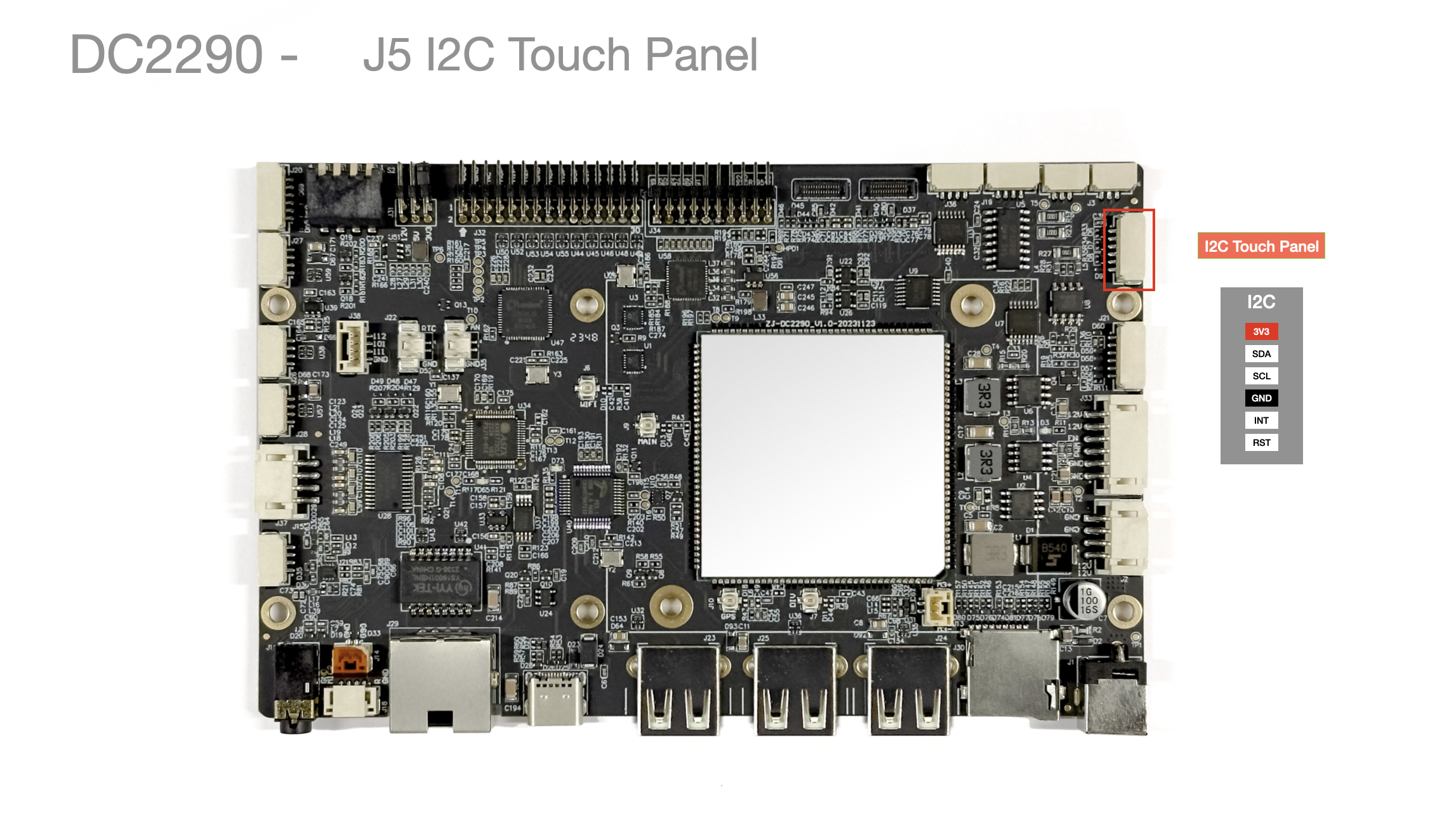
| Pin No. | Pin Description | Notes |
|---|---|---|
| 1 | 3V3 | |
| 2 | SDA 3 | |
| 3 | SCL 3 | |
| 4 | GND | Ground |
| 5 | INT | |
| 6 | RESET |
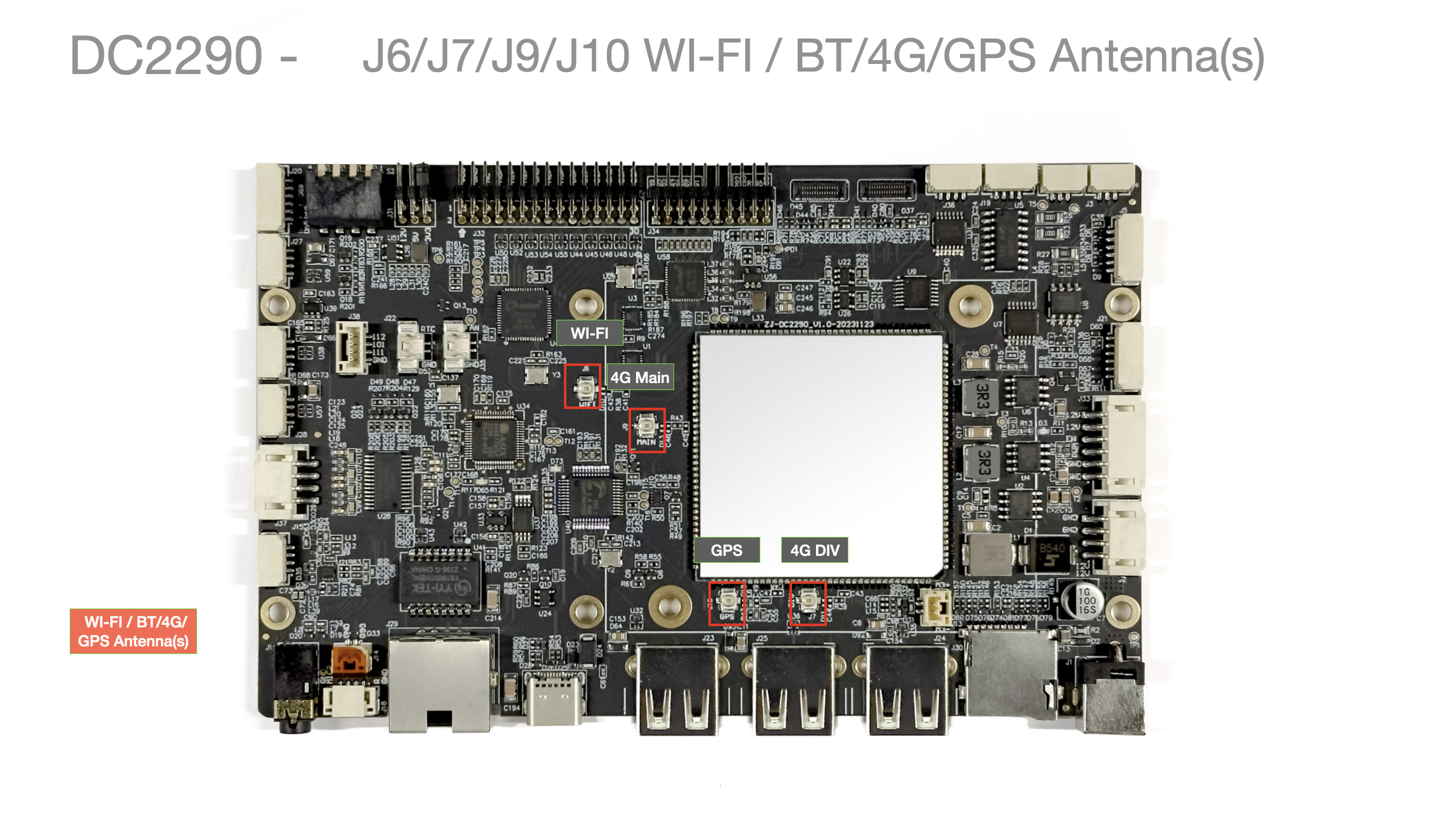
J6/J7/J9/J10 WI-FI / BT / 4G Antenna(s)
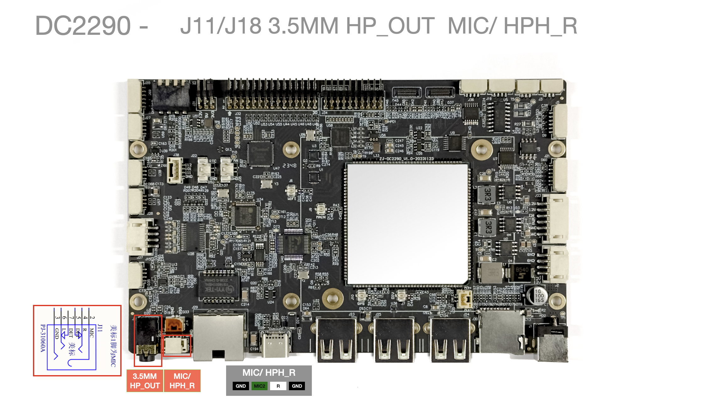
J11/J18 Headphone and Microphone Jacks (MIC, HPH_R)
J12 TYPE-C Multifunctional Port
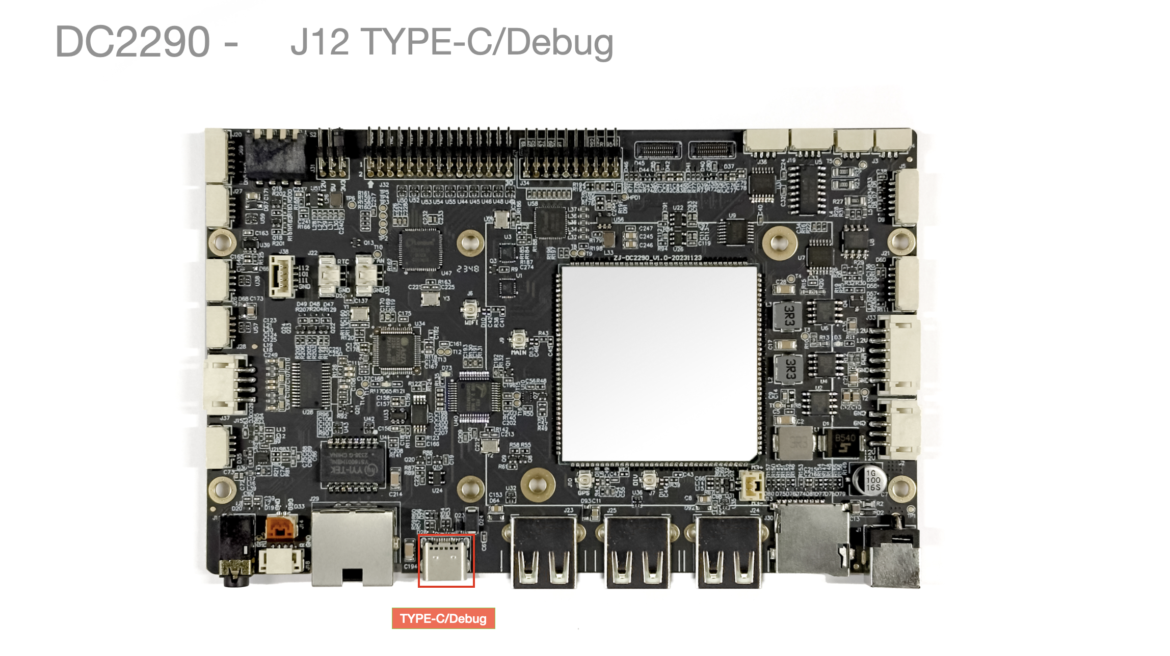
- TYPE-C Port: Debug
J13 MIC_3 Interface
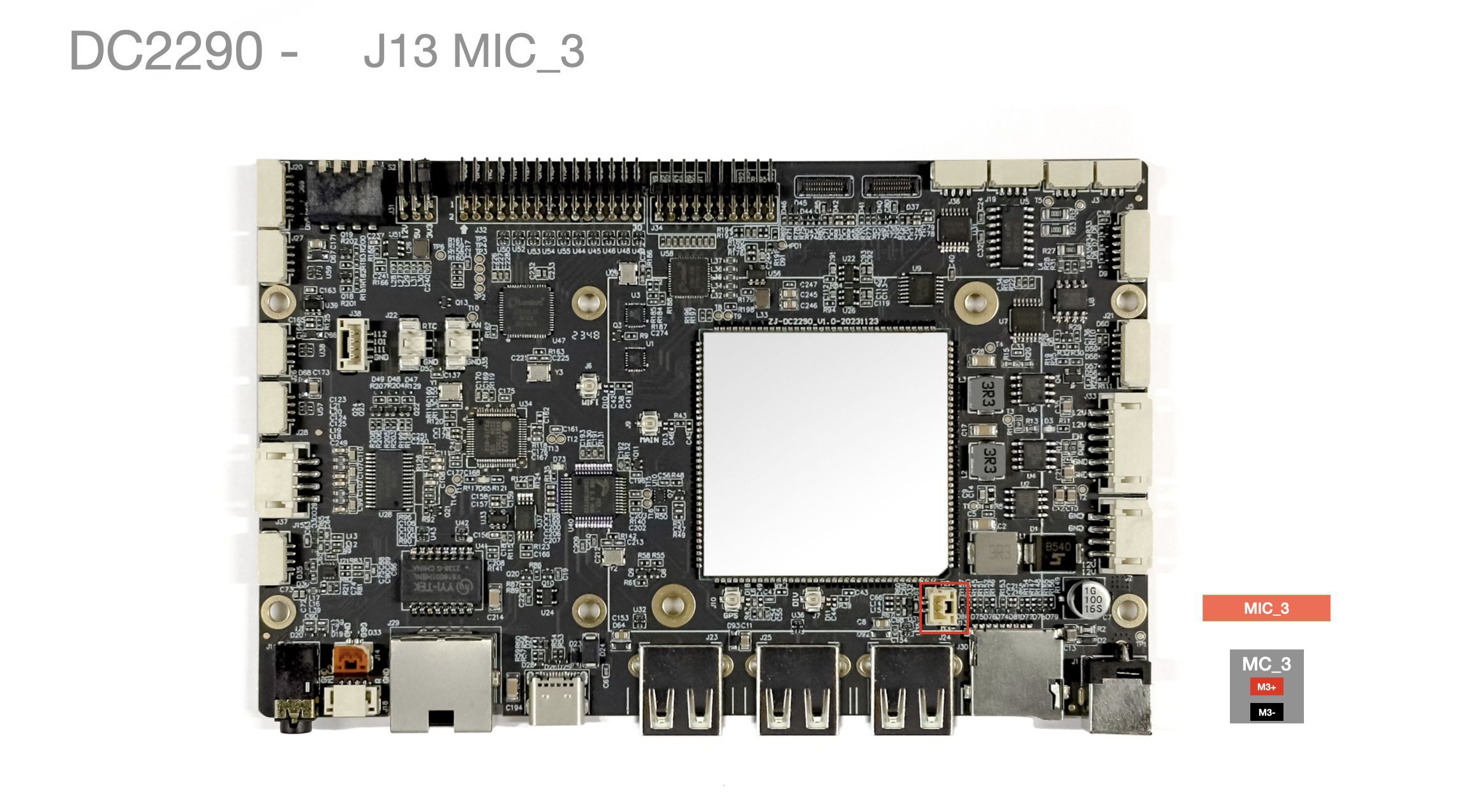
| Pin No. | Pin Description | Notes |
|---|---|---|
| 1 | MIC3A_P | |
| 2 | MIC3A_N |
J14 GPIO_99 Interface
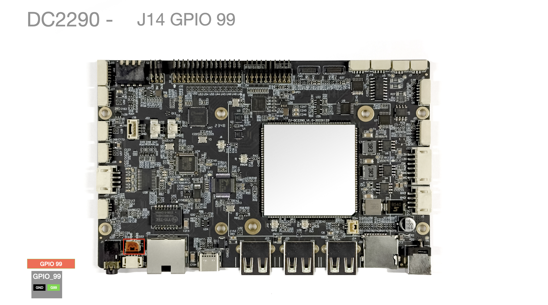
| Pin No. | Pin Description | Notes |
|---|---|---|
| 1 | GPIO_99 | |
| 2 | GND |
J15 MIC_1 and Earpiece Interface
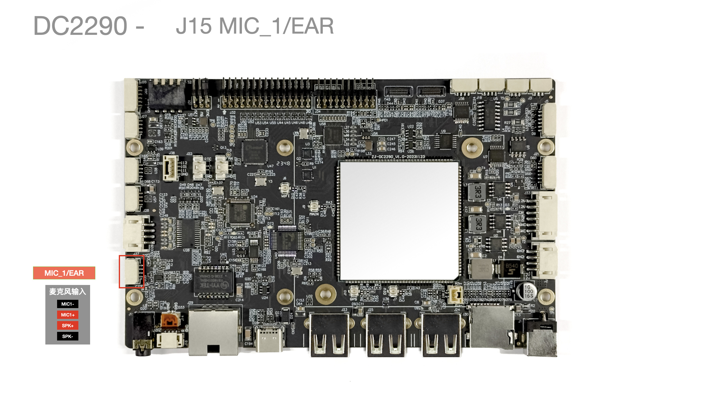
| Pin No. | Pin Description | Notes |
|---|---|---|
| 1 | EAR_N | |
| 2 | EAR_P | |
| 3 | MIC1A_P | |
| 4 | MIC1A_N |
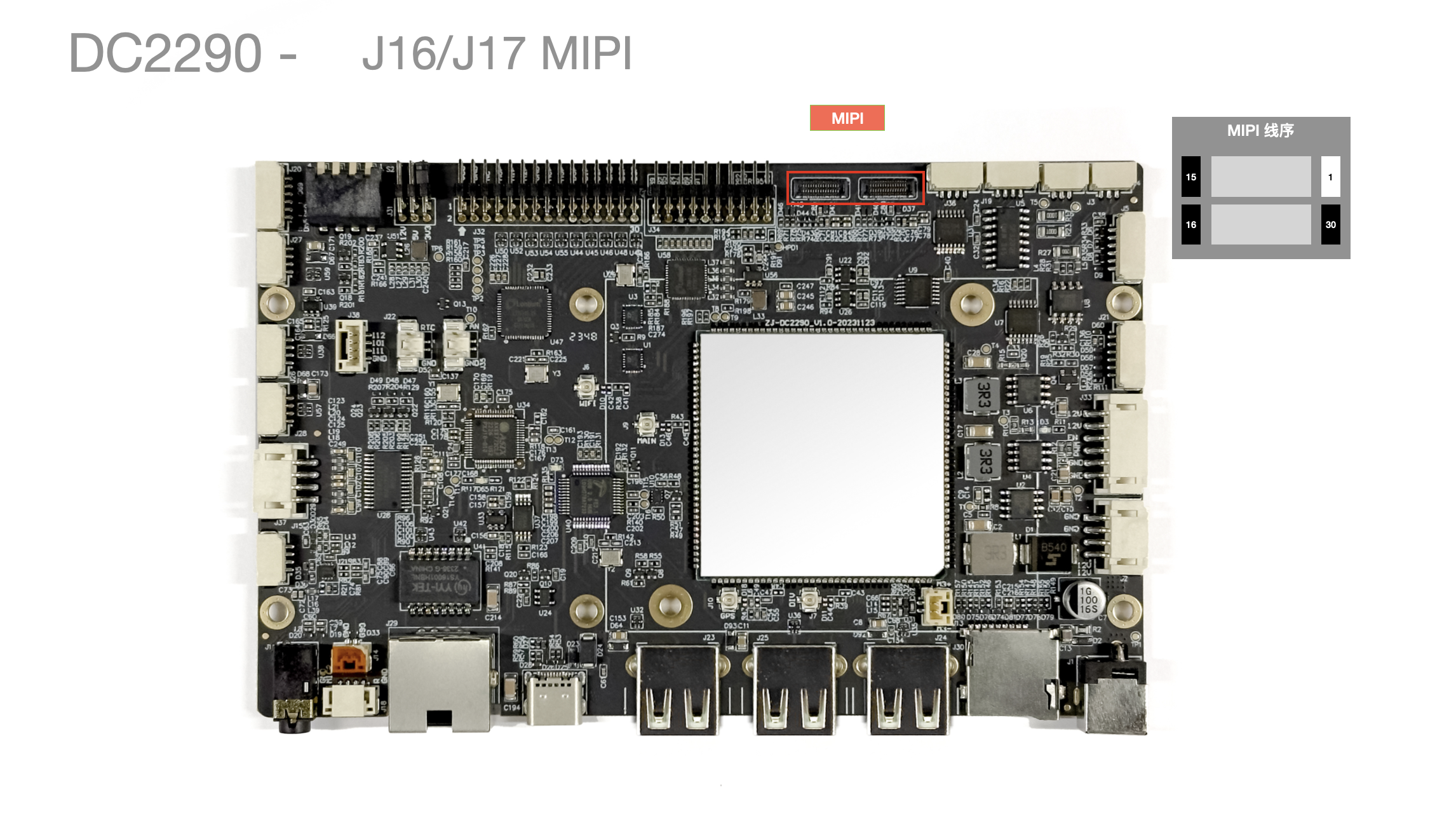
J16/J17 MIPI Camera Interfaces
J20 Buttons
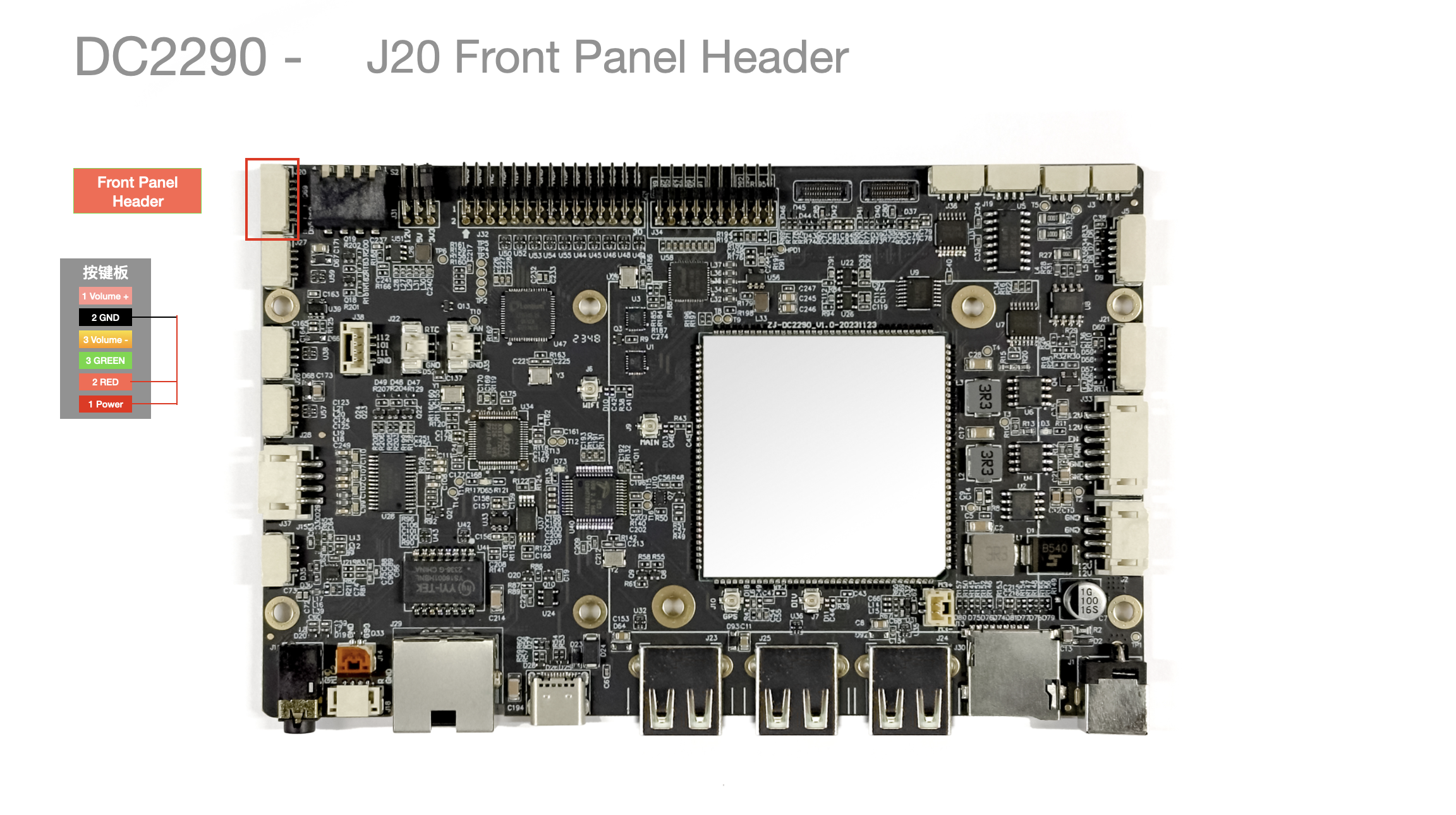
| Pin No. | Pin Description | Notes |
|---|---|---|
| 1 | PWRKEY | |
| 2 | GPIO_107_3 | |
| 3 | GPIO_4P_3 | |
| 4 | KEY_VOL_DOWN | |
| 5 | GND | |
| 6 | KEY_VOL_UP |
J21 SIM_2 Card Expansion
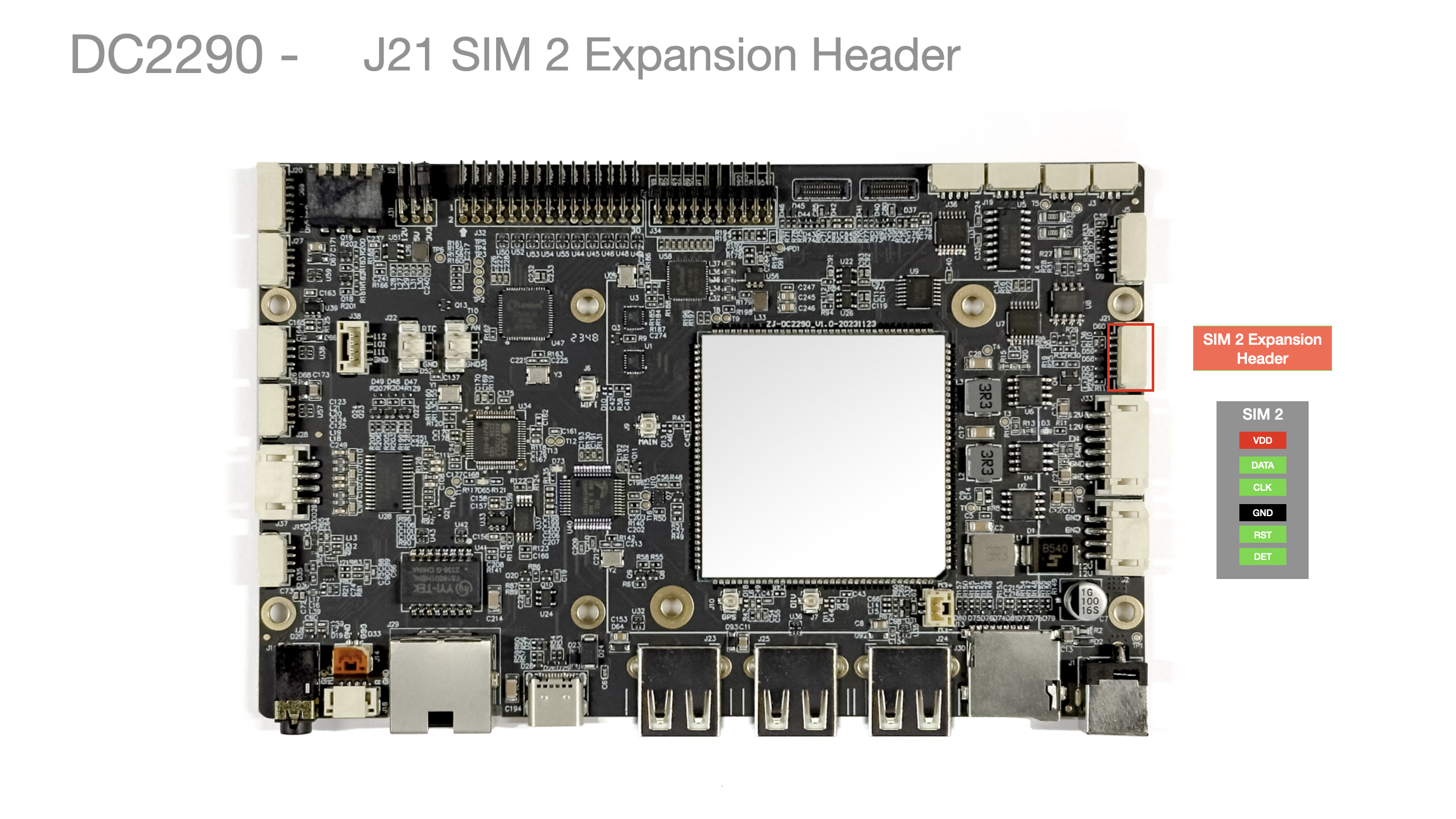
| Pin No. | Pin Description | Notes |
|---|---|---|
| 1 | USIM2_VDD | |
| 2 | USIM2_DATA | |
| 3 | USIM2_CLK | |
| 4 | GND | |
| 5 | USIM2_RST | |
| 6 | USIM2_DET |
J22 RTC Battery
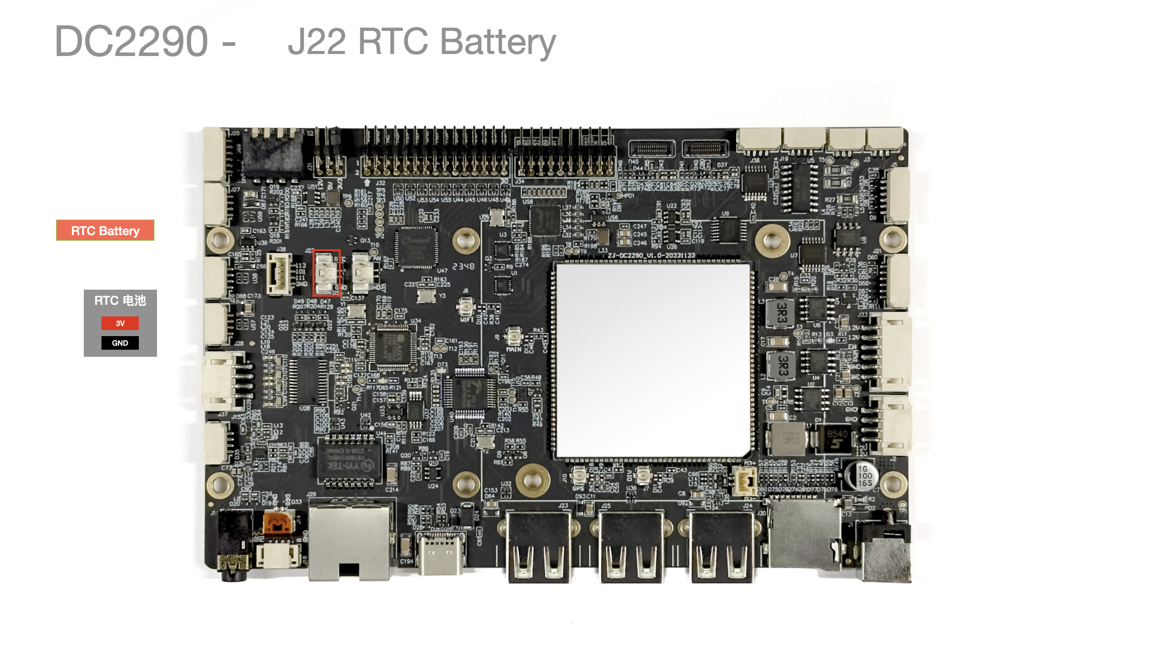
| Pin No. | Pin Description | Notes |
|---|---|---|
| 1 | RTC 3V | |
| 2 | GND |
J23/J24/J25 USB-A
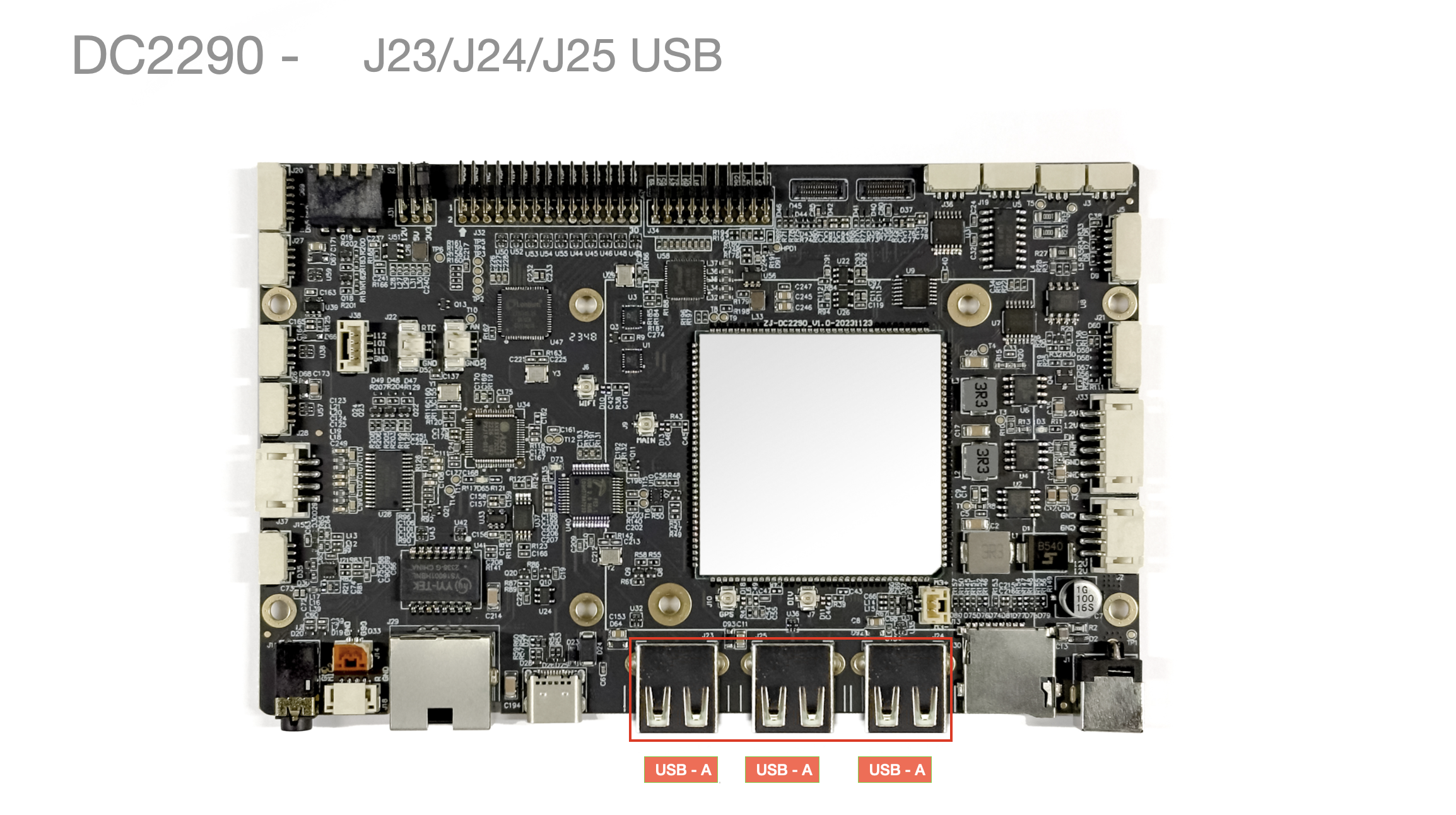
- Standard USB-A
J23/J24/J25 USB Ports
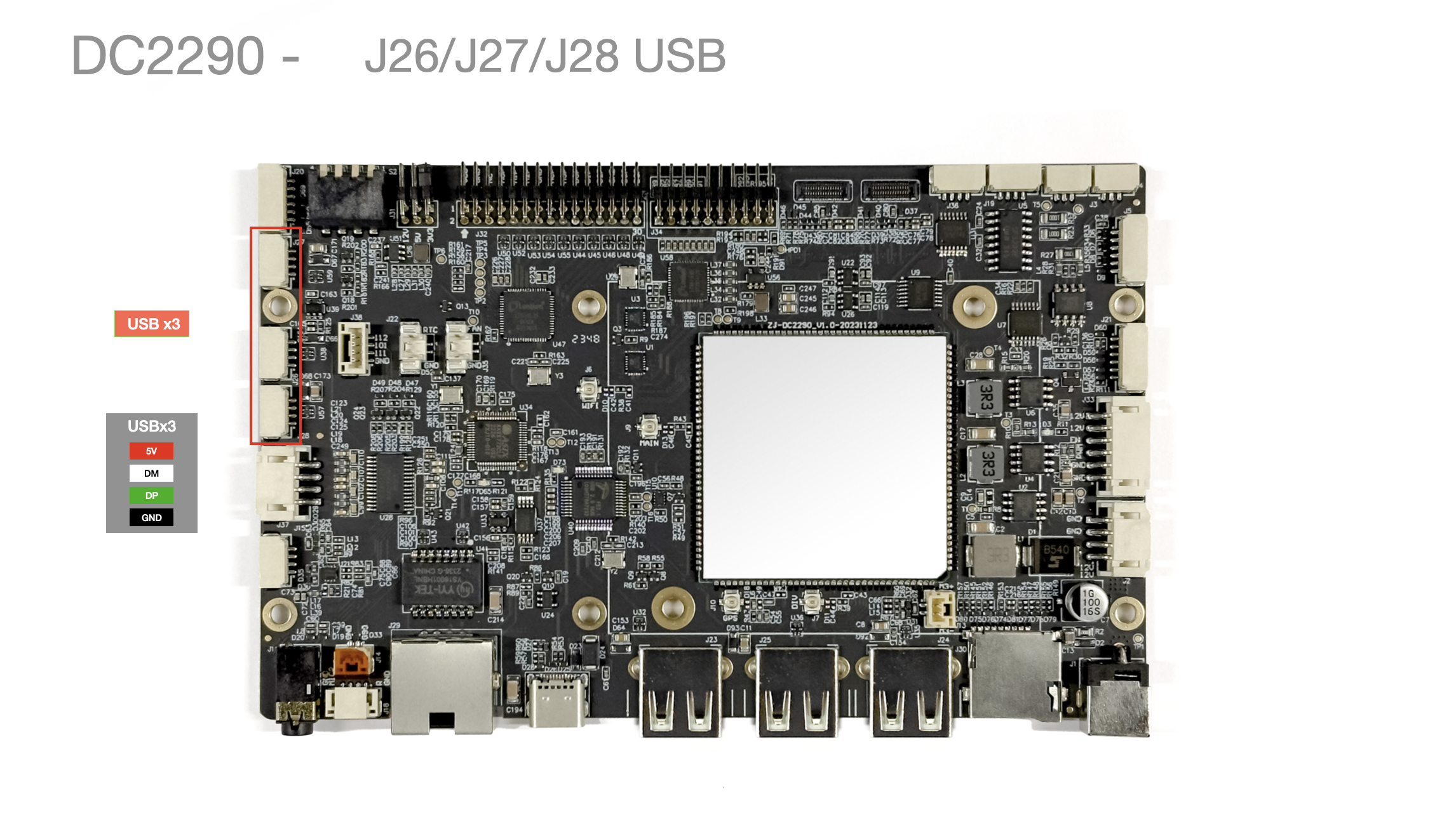
| Pin No. | Pin Description | Notes |
|---|---|---|
| 1 | GND | |
| 2 | USBA_P | |
| 3 | USBA_N | |
| 4 | 5V |
J29 Ethernet Port
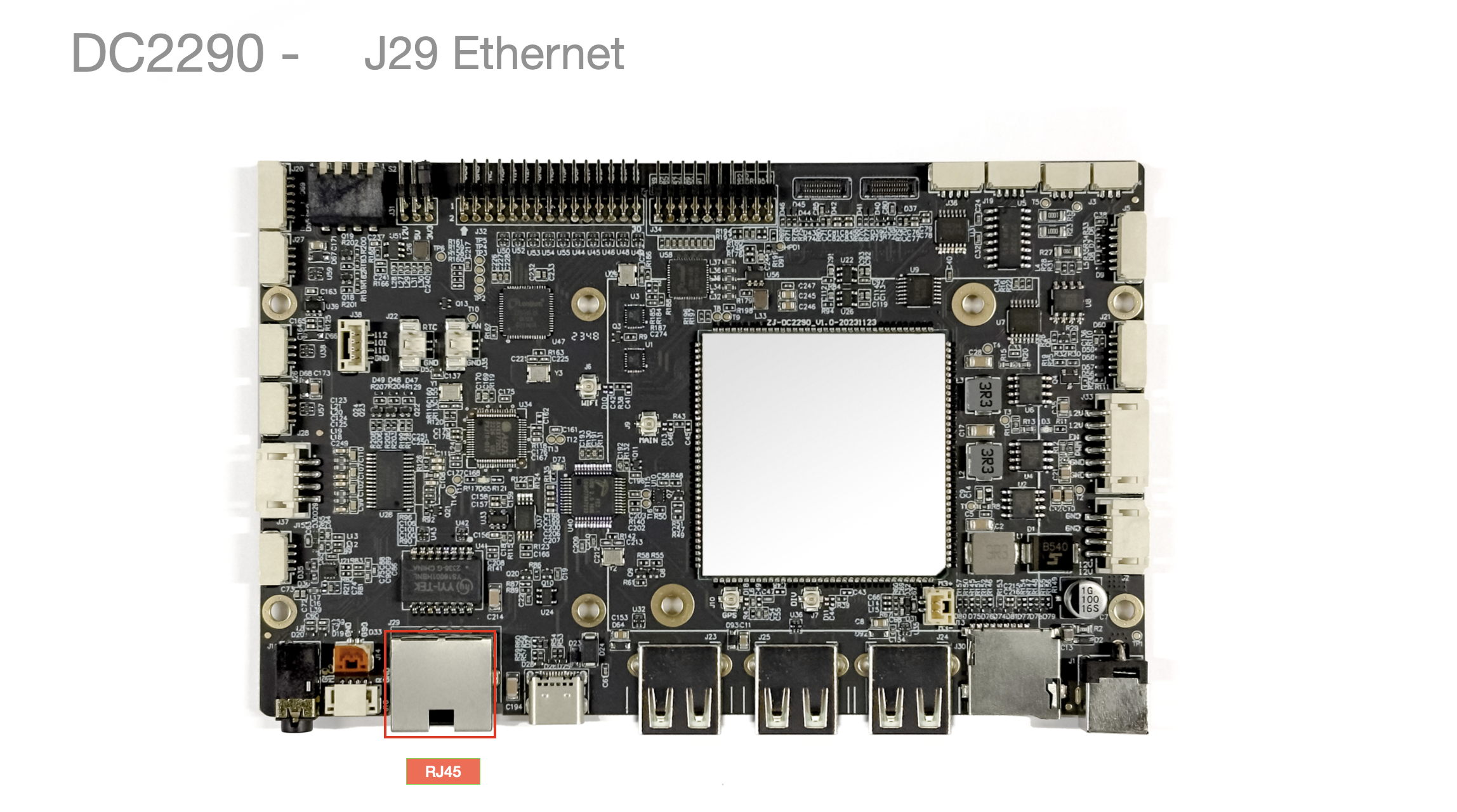
- 10M/100M Ethernet
J30 SD-CARD Slot
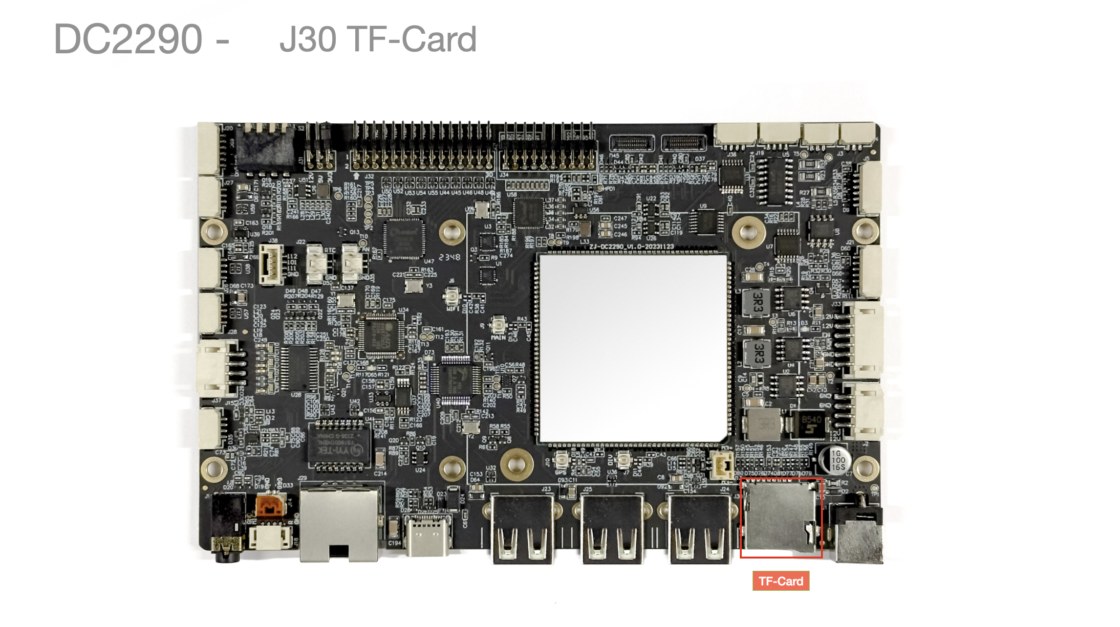
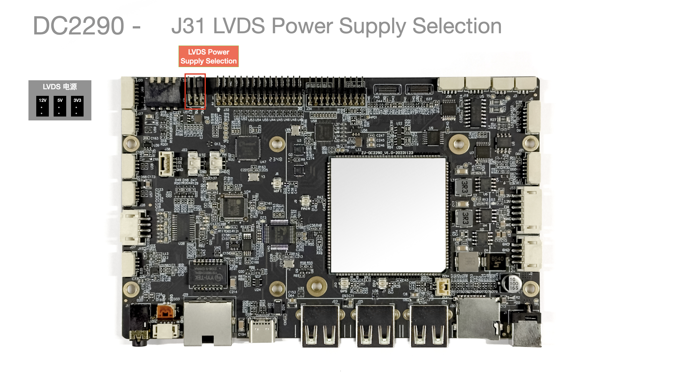
J31 LVDS Power Supply Selection Interface
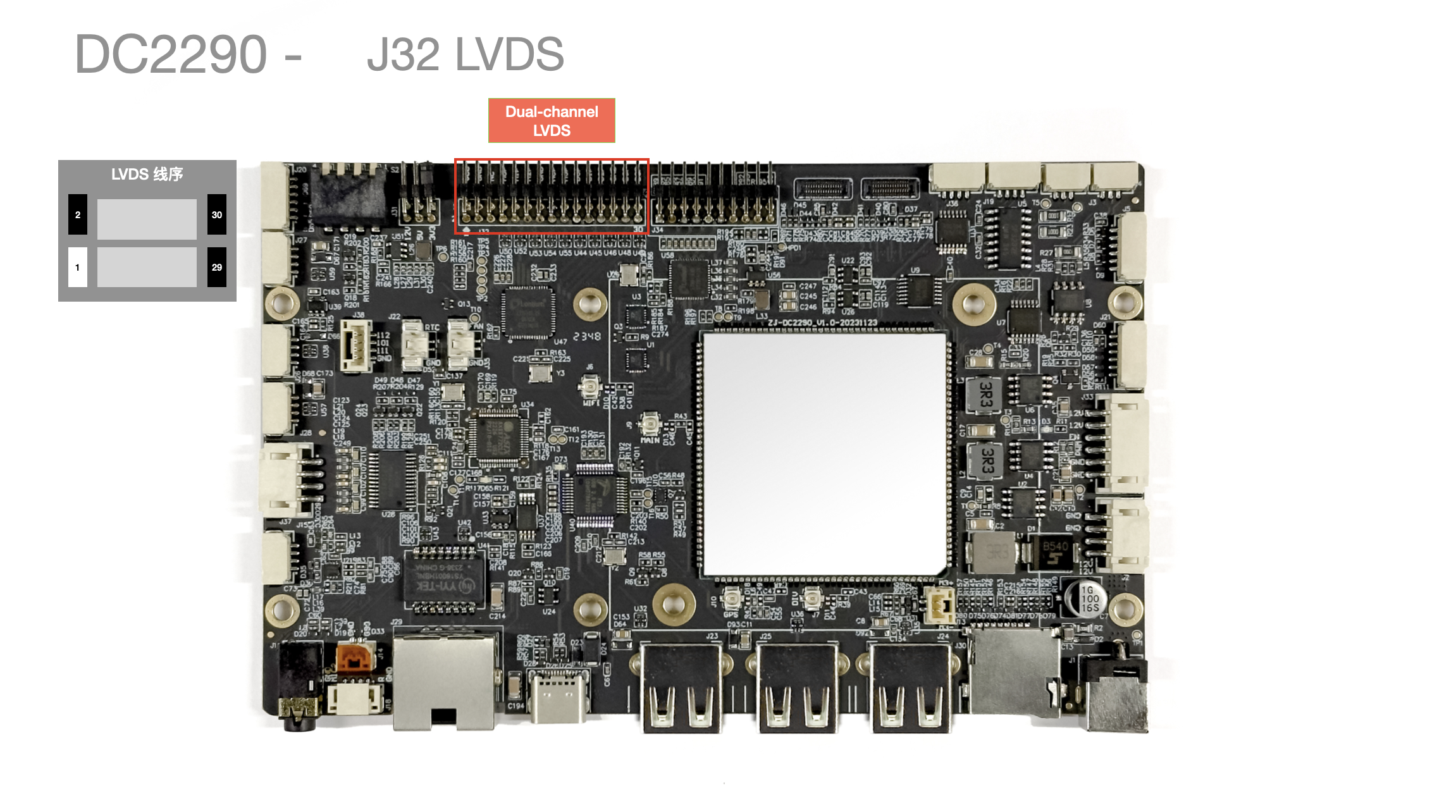
J32: LVDS Screen Interface
J33: Screen Backlight Interface
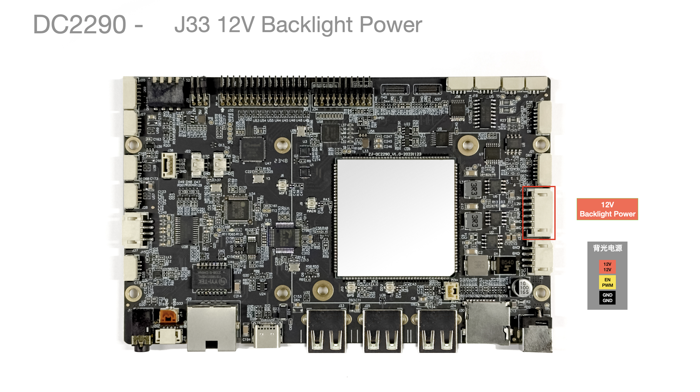
| Pin No. | Pin Description | Notes |
|---|---|---|
| 1 | 12V | |
| 2 | 12V | |
| 3 | BL1_EN | |
| 4 | BL1_PWM | |
| 5 | GND | |
| 6 | GND |
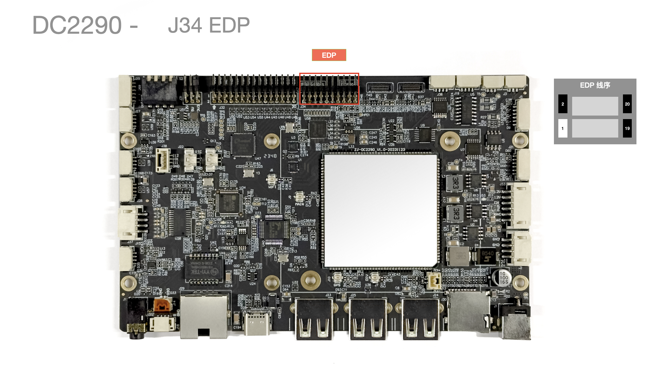
J34 EDP Screen Interface
J35/J36/J38 GPIO Interfaces
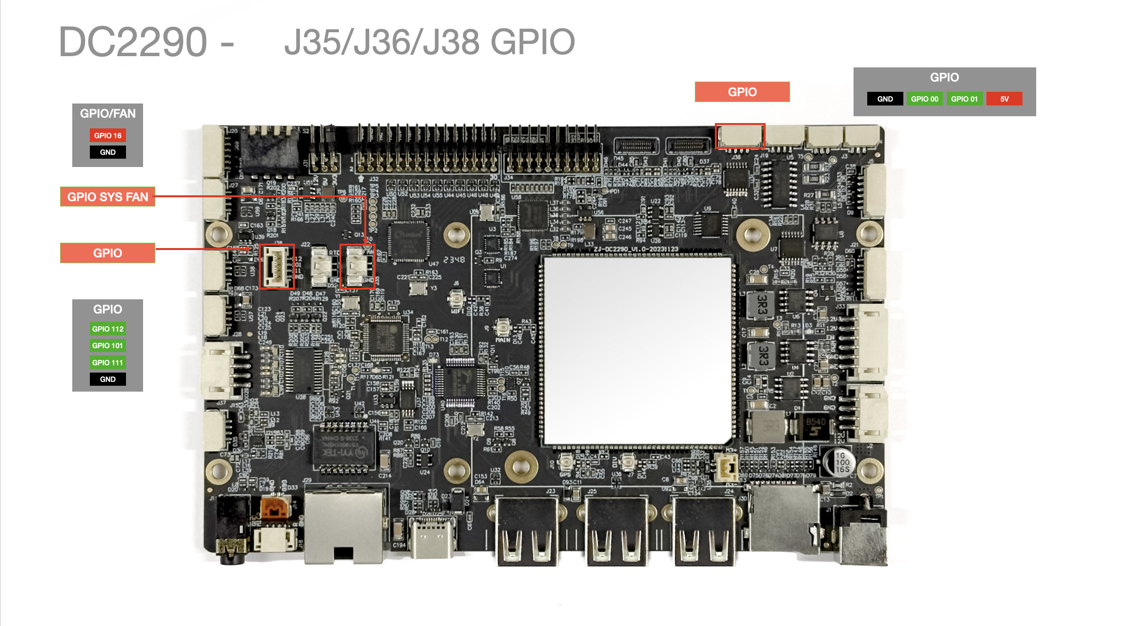
| Pin No. | Pin Description | Notes |
|---|---|---|
| J35_1 | GPIO_16 | |
| J35_2 | GND | |
| J36_1 | GND | |
| J36_2 | GPIO_00 | |
| J36_3 | GPIO_01 | |
| J36_4 | 5V | |
| J38_1 | GPIO_112 | |
| J38_2 | GPIO_101 | |
| J38_3 | GPIO_111 | |
| J38_4 | GND |
J37 AUDIO_OUT Interface
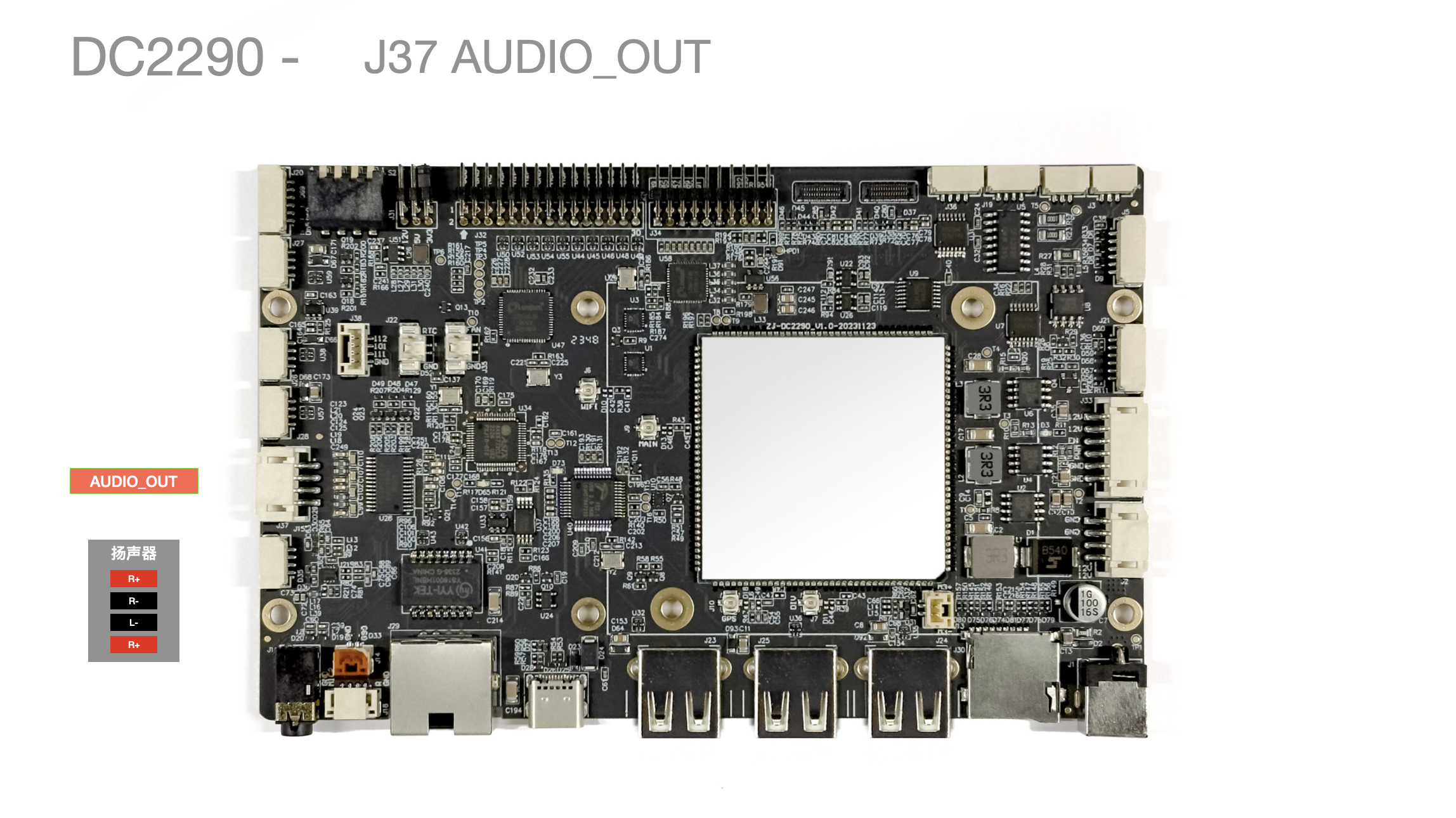
| Pin No. | Pin Description | Notes |
|---|---|---|
| 1 | L+ | |
| 2 | L- | |
| 3 | R+ | |
| 4 | R- |
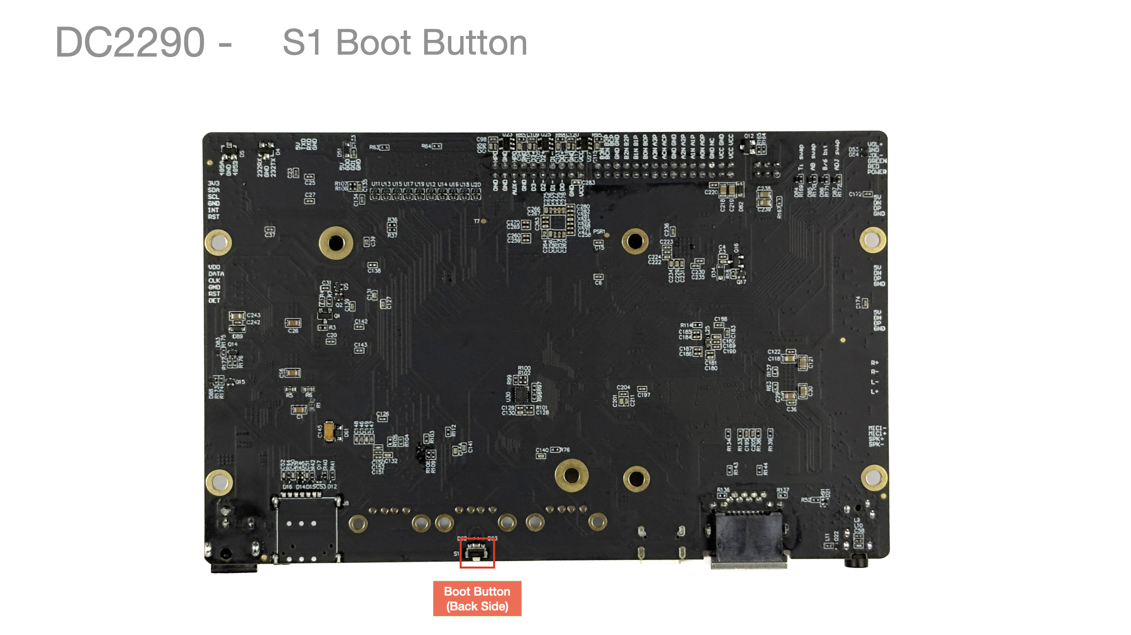
S1 Boot Button
-
Located below the J25 USB interface, used to enter burning mode.
-
Usage: Press and hold this button before powering on, then release after powering on to enter burning mode.
S2 LVDS Screen Configuration
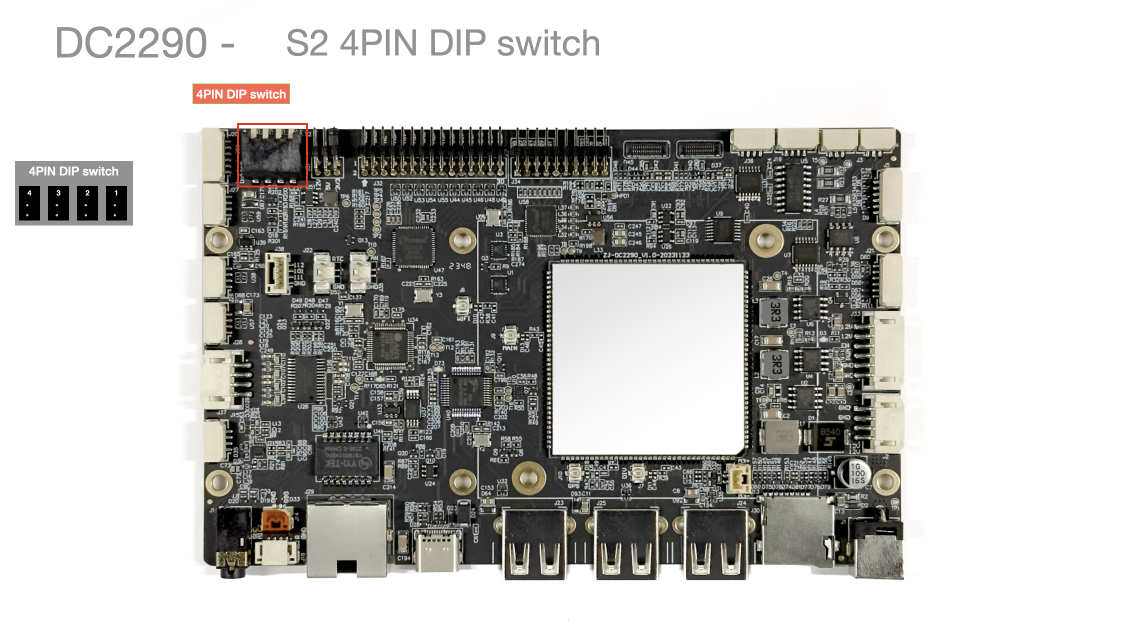
| Pin No. | Pin Description | Notes |
|---|---|---|
| 1 | GPIO102 | LVDSTX_DATAFORMAT |
| 2 | GPIO103 | LVDSTX_PORT_SWAP |
| 3 | GPIO104 | LVDSTX_COLORDEPTH |
| 4 | GPIO105 | LVDS Backlight Polarity Adjustment |