Expansion Board 24PIN - CAM126 (RV1126)

The CAM126B-P-24 expansion board can also be connected to CAM126 (RV1126) through a 24PIN 0.5mm FPC cable. The 24PIN signal definition is identical on both platforms, but the GPIO numbers, SDIO/UART controllers, and device nodes are different, so the 1126B-P software configuration cannot be reused directly.
Caution
CAM126 and CAM126B-P are different platforms. Chips, firmware, and software are not compatible with each other.
- The 24PIN SDIO interface is 1.8V. Before connecting, make sure the VCCIO domain feeding
GPIO1on the RV1126 side is also 1.8V; if it is 3.3V, change the voltage or add level shifters. - The RV1126 SDK does not include the AIC8800 driver. You need to match it yourself; see Wi-Fi / Bluetooth Debugging.
- For the RV1126 dts and pin configuration, see RV1126 24PIN Configuration.
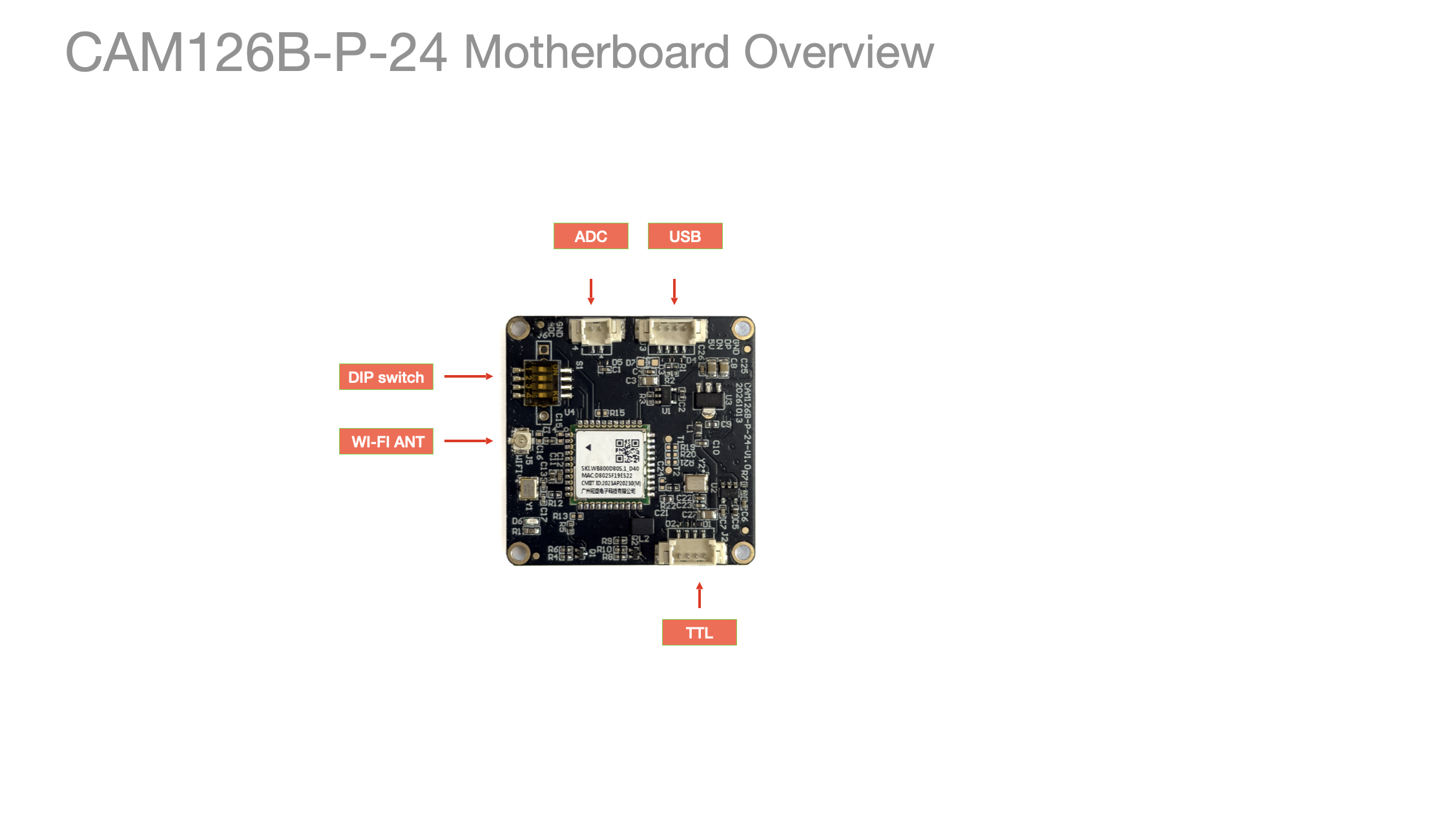
Expansion Board Interface
Installation
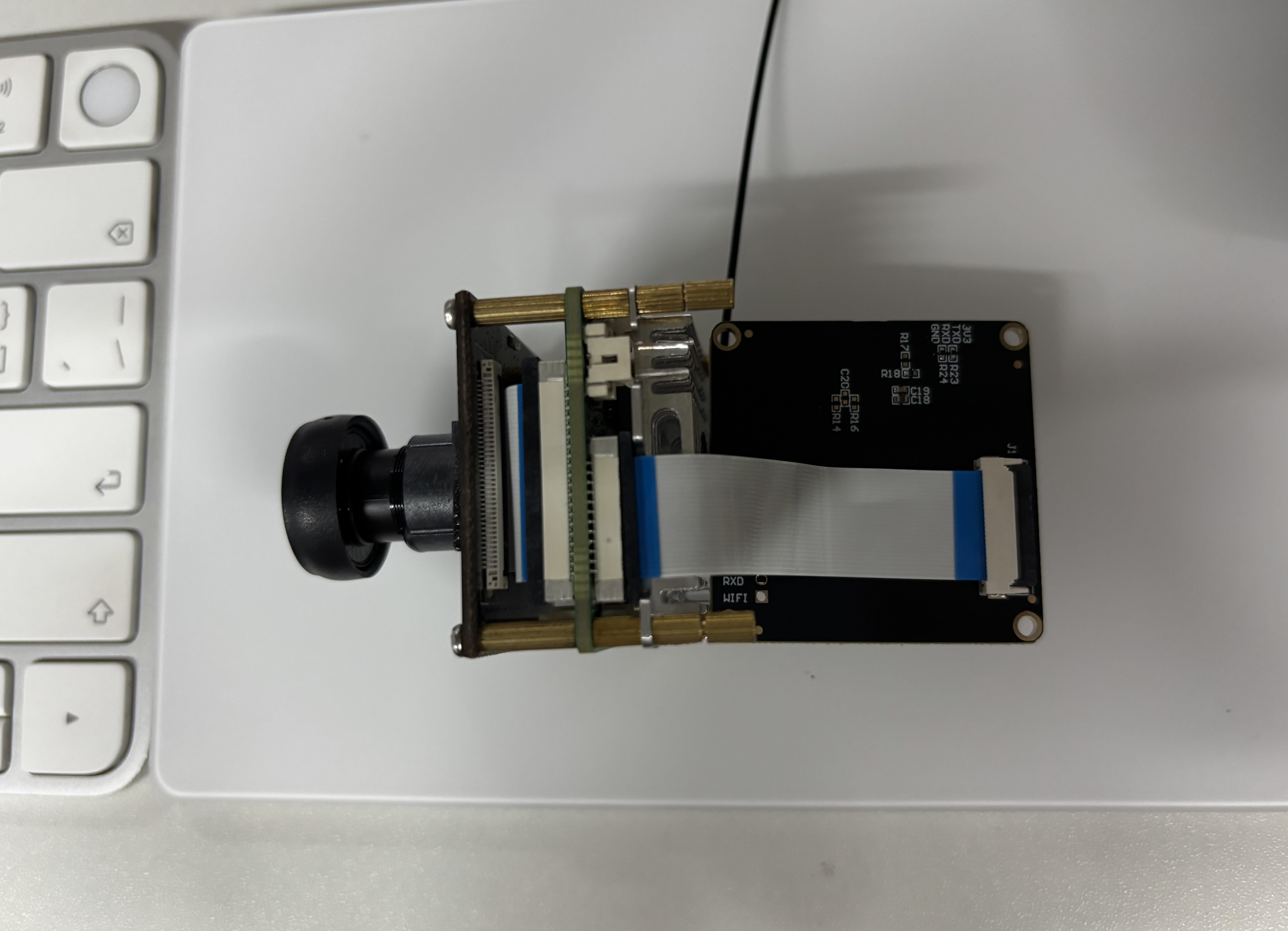
- Pressing down the black latch on the expansion board locks the FPC cable; lifting it releases the cable.
J1 24PIN FPC
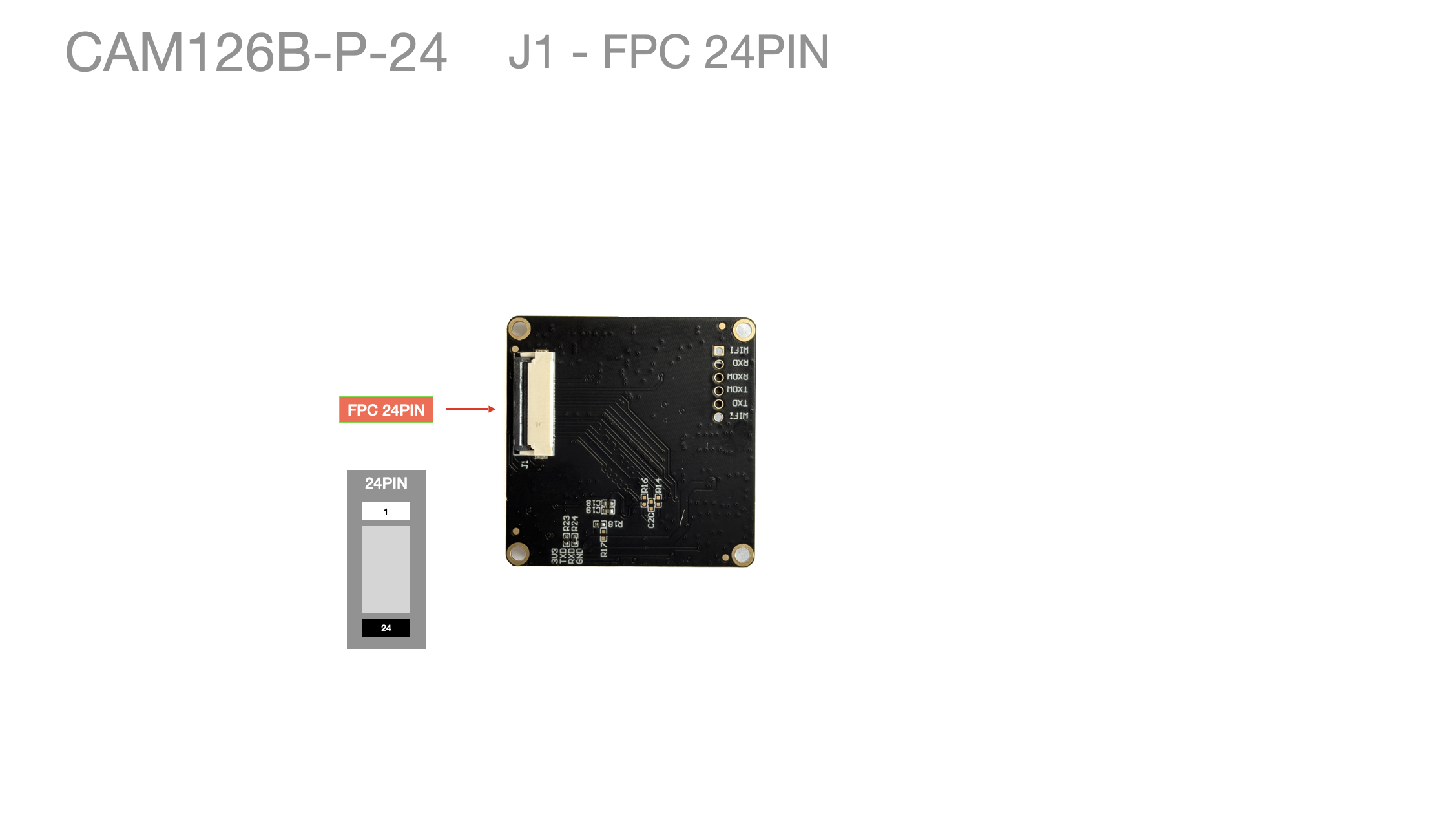
24 PIN 0.5MM FPC connector, model
X05C2024TZ
24PIN Definition and RV1126 Pins
| pin | Definition | RV1126 GPIO | RV1126 Notes | RV1126B-P GPIO |
|---|---|---|---|---|
| 1 | GND | |||
| 2 | GND | |||
| 3 | VCC5V0 | Expansion board power | ||
| 4 | VCC5V0 | Expansion board power | ||
| 5 | USB_HOST_DP | Y1 | USB Host D+ | |
| 6 | USB_HOST_DM | Y2 | USB Host D- | |
| 7 | GND | |||
| 8 | ADKEY_IN0 | E17 | SARADC_IN0 | |
| 9 | GND | |||
| 10 | WIFI_WAKE_HOST | GPIO1_D1 | Wi-Fi wakes host | GPIO3_B7 |
| 11 | BT_RST | GPIO3_A5 | Bluetooth reset | GPIO6_A1 |
| 12 | BT_WAKE | GPIO3_A6 | Host wakes Bluetooth | GPIO6_A2 |
| 13 | BT_WAKE_HOST | GPIO3_A4 | Bluetooth wakes host | GPIO6_A0 |
| 14 | WIFI_REG_ON | GPIO1_D0 | Wi-Fi power enable | GPIO3_B6 |
| 15 | SDIO_D0 | GPIO1_B4 | sdio func 1 | GPIO3_A2 |
| 16 | SDIO_D1 | GPIO1_B5 | sdio func 1 | GPIO3_A3 |
| 17 | SDIO_D2 | GPIO1_B6 | sdio func 1 | GPIO3_A4 |
| 18 | SDIO_D3 | GPIO1_B7 | sdio func 1 | GPIO3_A5 |
| 19 | SDIO_CMD | GPIO1_B3 | sdio func 1 | GPIO3_A1 |
| 20 | SDIO_CLK | GPIO1_B2 | sdio func 1 | GPIO3_A0 |
| 21 | UART0_RTSN | GPIO1_C0 | uart0 func 1 | GPIO3_A6 |
| 22 | UART0_TX | GPIO1_C3 | uart0 func 1, 1.8V | GPIO3_B1 |
| 23 | UART0_RX | GPIO1_C2 | uart0 func 1, 1.8V | GPIO3_B0 |
| 24 | UART0_CTSN | GPIO1_C1 | uart0 func 1 | GPIO3_A7 |
RV1126 side mapping:
| Function | RV1126 Controller | Device Node | 1126B-P Reference |
|---|---|---|---|
| SDIO | sdio@ffc70000 (mmc1) | mmc1 under /sys/bus/mmc/devices | sdmmc1 (mmc2) |
| Bluetooth UART | uart0@ff560000 (serial0) | /dev/ttyS0 | uart2 (/dev/ttyS2) |
| Wi-Fi power enable | GPIO1_D0 | Controlled by sdio_pwrseq | GPIO3_B6 |
| Wi-Fi wake host | GPIO1_D1 | WIFI,host_wake_irq | GPIO3_B7 |
| Bluetooth reset | GPIO3_A5 | BT,power_gpio | GPIO6_A1 |
Pin sources: 1126-1126BP-24pin.xlsx, 1126pin2pin1126BP-GPIO.xlsx
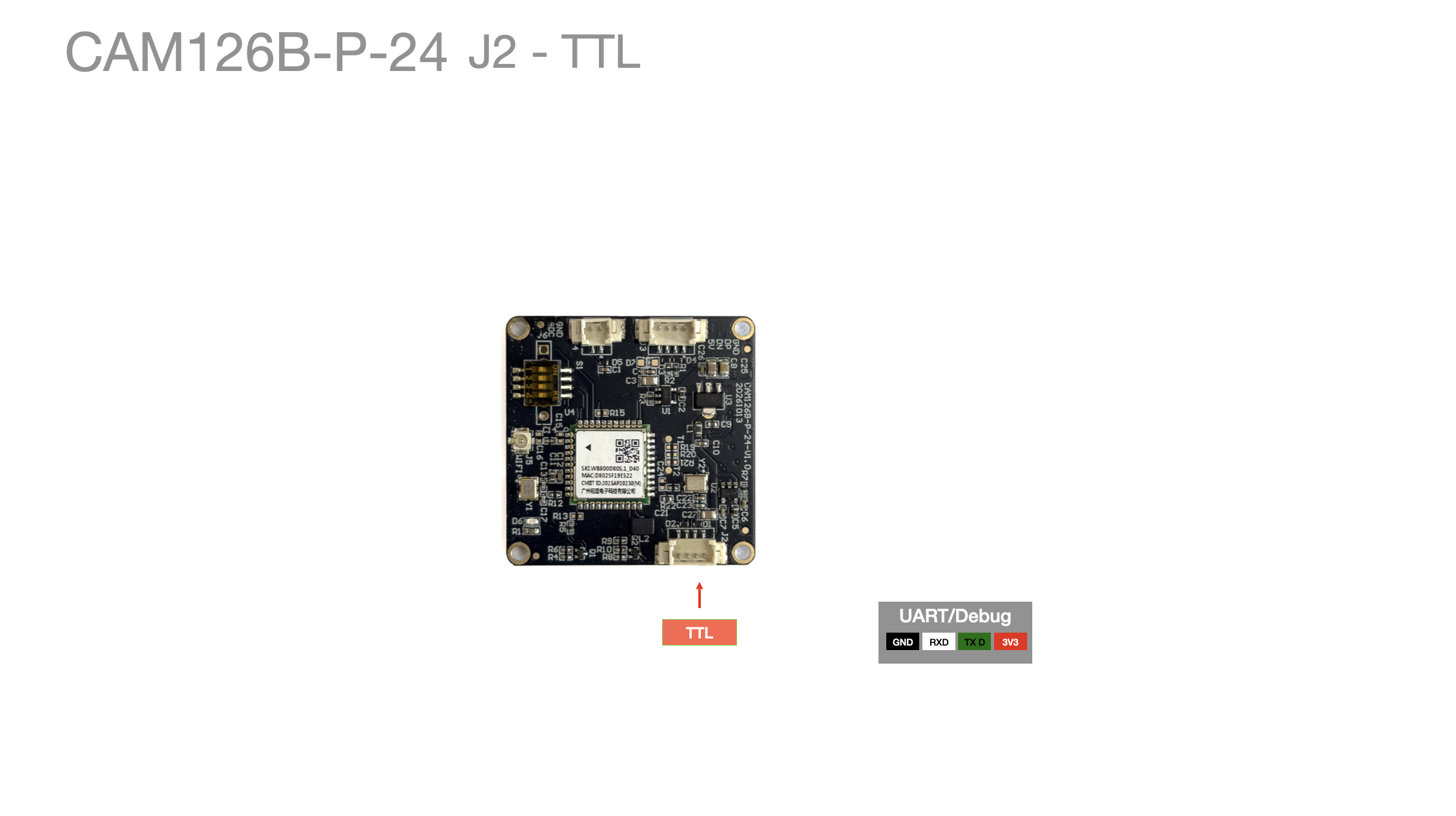
J2 TTL
Information
When using TTL, set the S01 DIP switch to 2 / 4.
| Item | Value |
|---|---|
| Device node | /dev/ttyS0 (RV1126 uart0) |
| Controller | uart0 @ 0xff560000 (alias serial0 = &uart0) |
| TX | 24PIN-22 UART0_TX = GPIO1_C3 |
| RX | 24PIN-23 UART0_RX = GPIO1_C2 |
| RTS / CTS | 24PIN-21 = GPIO1_C0 / 24PIN-24 = GPIO1_C1 |
| Default baud rate | 9600 |
J3 USB
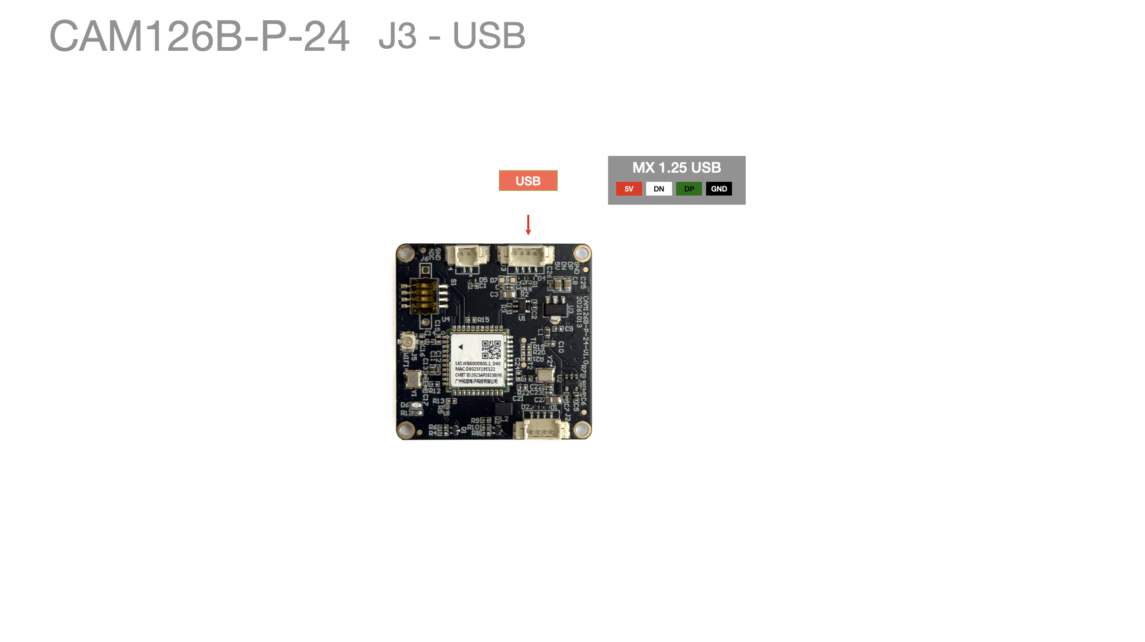
| Pin No. | Function | Reference Color |
|---|---|---|
| 1 | GND | Black |
| 2 | OTG_DP | Green-white |
| 3 | OTG_DM | White |
| 4 | VCC5V0 | Red |
J4 Native ADC Interface
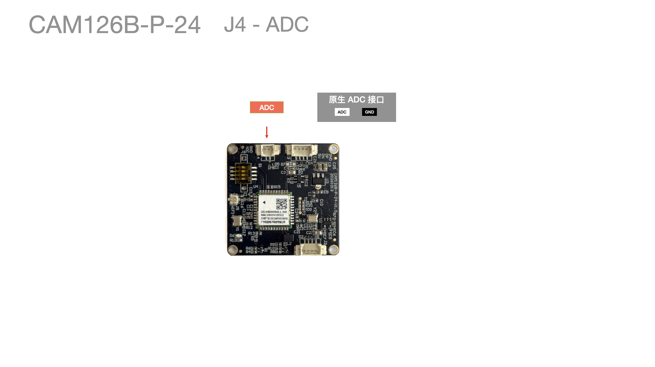
| Pin No. | Function | Reference Color |
|---|---|---|
| 1 | GND | Black (ADC function TBD) |
| 2 | ADC | Red (ADC function TBD) |
J5 WIFI Antenna
Information
When using Wi-Fi / Bluetooth, set the S01 DIP switch to 1 / 3.
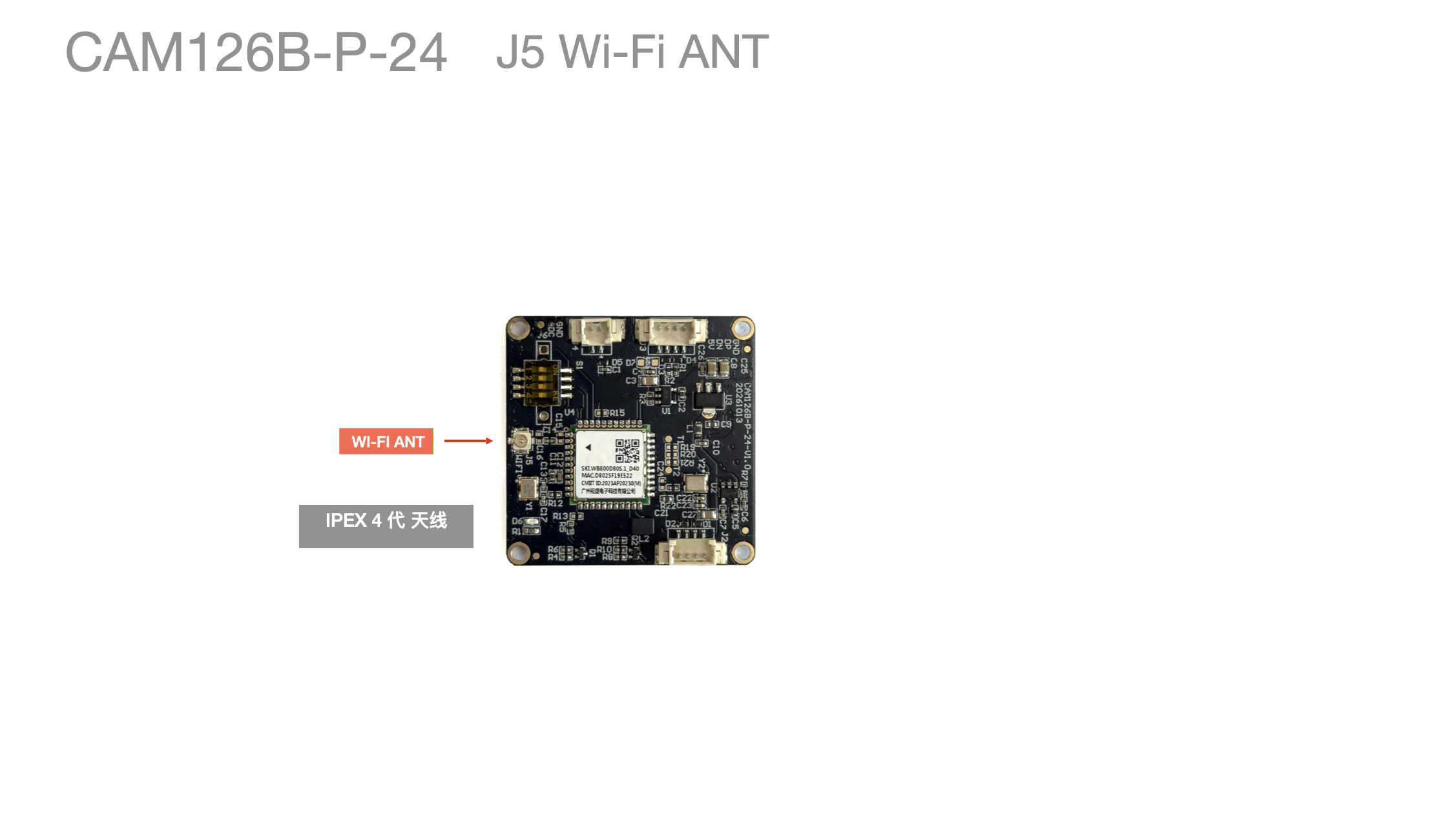
- Wi-Fi / BT antenna - IPEX generation 4
S01 DIP Switch
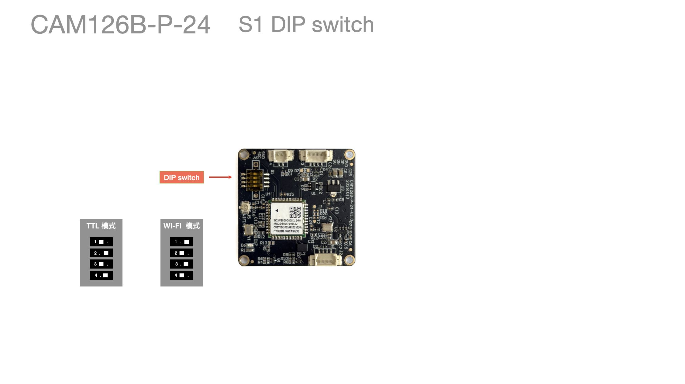
| Pin No. | Function | Description |
|---|---|---|
| 1 | UART RX WIFI | 1 / 3 on: UART connected to the Wi-Fi / BT module |
| 2 | UART RX TTL | 2 / 4 on: UART connected to 24PIN TTL debugging |
| 3 | UART TX WIFI | 1 / 3 on: UART connected to the Wi-Fi / BT module |
| 4 | UART TX TTL | 2 / 4 on: UART connected to 24PIN TTL debugging |
Schematic
| Item | Link |
|---|---|
| RV1126 38x38 schematic | RV1126_38X38_230926原理图.pdf |
| CAM126B-P-24 expansion board schematic | CAM126B-P-24-V1.0-20261013-原理图.pdf |
| 24PIN mapping table | 1126-1126BP-24pin.xlsx |
| GPIO mapping table | 1126pin2pin1126BP-GPIO.xlsx |
For the complete RV1126 dts, driver matching, and verification flow, see: